System-in-package device and method

A system-level packaging and device technology, which is applied in the manufacture of electrical solid-state devices, semiconductor devices, semiconductor/solid-state devices, etc., can solve problems such as separation of metal layer chips, abnormal product quality, and extremely high process precision requirements, so as to improve yield rate, Improve the heat dissipation effect and simplify the process

Pending Publication Date: 2021-11-19
NANTONG FUJITSU MICROELECTRONICS
View PDF0 Cites 0 Cited by
  • Summary
  • Abstract
  • Description
  • Claims
  • Application Information

AI Technical Summary

Problems solved by technology

[0004] However, embedded packaging technology usually covers a layer of metal layer on both sides of the chip, and then forms a metal groove by electroplating on the metal layer. During the production process, the metal layer is easily separated from the chip due to external force impact. resulting in abnormal product quality
Embedded packaging technology has extremely high requirements on process precision, and currently there are few substrate manufacturers that can undertake it, and most of them can only embed smaller devices such as capacitors and resistors.

Method used


Image

  • System-in-package device and method
  • System-in-package device and method
  • System-in-package device and method

Examples


Embodiment Construction

[0025] The following will clearly and completely describe the technical solutions in the embodiments of the present application with reference to the drawings in the embodiments of the present application. Obviously, the described embodiments are only some of the embodiments of the present application, not all of them. Based on the embodiments in this application, all other embodiments obtained by persons of ordinary skill in the art without making creative efforts belong to the scope of protection of this application.

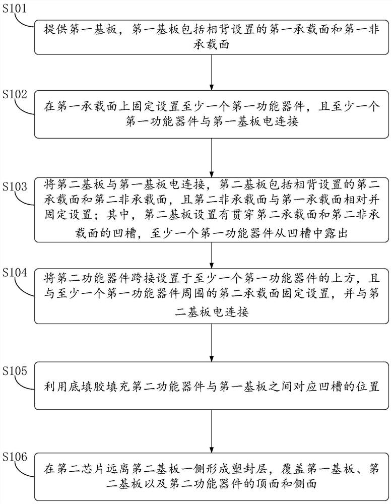
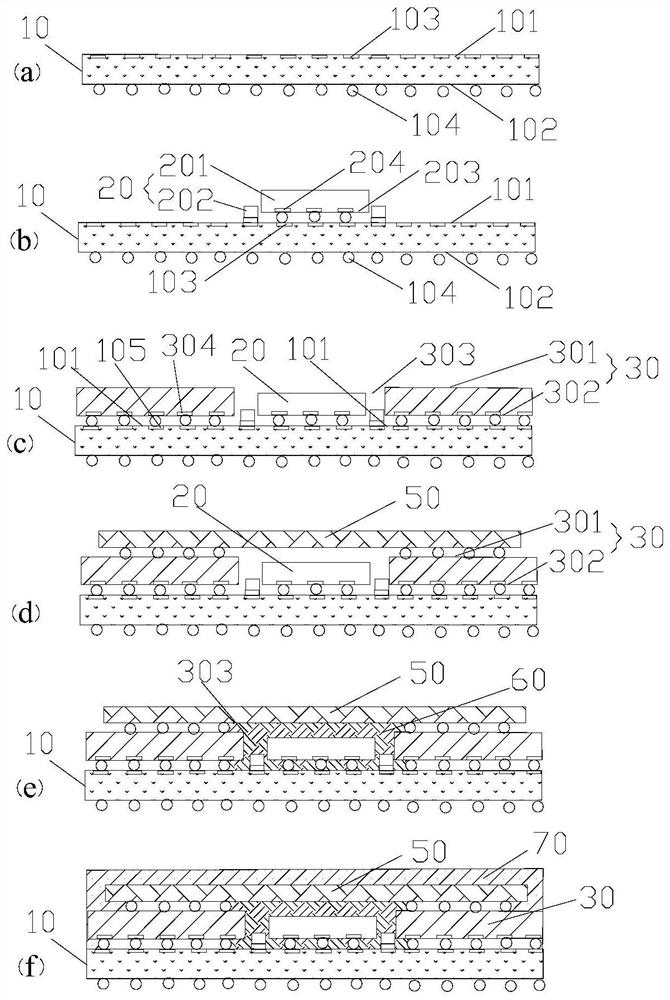
[0026] see figure 1 and figure 2 , figure 1 is a schematic flow chart of an embodiment of the system-in-package method of the present application, figure 2 yes figure 1 Steps S101-Step S106 correspond to a schematic structural diagram of an embodiment, and the packaging method provided in this application includes:

[0027] S101 : providing a first substrate 10 , the first substrate 10 includes a first bearing surface 101 and a first non-bearing surface ...


PUM


Abstract

The invention discloses a system-in-package device and method. The device comprises: a first substrate comprising a first bearing surface and a first non-bearing surface, wherein the first bearing surface and the first non-bearing surface are arranged in a back-to-back manner; at least one first functional device fixed on the first bearing surface and electrically connected with the first substrate; a second substrate electrically connected with the first substrate and comprising a second bearing surface and a second non-bearing surface, wherein the second bearing surface and the second non-bearing surface are oppositely arranged, the second non-bearing surface is opposite to the first bearing surface and is fixedly arranged, the second substrate is provided with a groove penetrating through the second bearing surface and the second non-bearing surface, and the at least one first functional device is exposed from the groove; and a second functional device arranged above the at least one first functional device in a bridging manner, fixedly arranged with the second bearing surface around the at least one first functional device, and electrically connected with the second substrate. In this way, the yield of the system-in-package device can be effectively improved.

Description

technical field [0001] The present application relates to the technical field of semiconductor packaging, in particular to a system-in-package device and method. Background technique [0002] As the development of Moore's Law is approaching the limit, the integration of integrated circuits is getting higher and higher, and electronic products are developing in the direction of miniaturization, intelligence and high performance. Among them, system-in-package technology is currently the mainstream technology that can realize system miniaturization. Different chips can be packaged side by side or stacked, and multiple active electronic devices or optional passive devices with different functions can be assembled together. In order to achieve a specific function. [0003] The structural design of system-in-package devices in the prior art is usually stacked horizontally or vertically on a single substrate. In order to further compress the packaging size, embedded packaging tec...

Claims


Application Information

Patent Timeline
Patent Type & Authority Applications(China)
IPC IPC(8): H01L23/488H01L21/60
CPCH01L23/488H01L24/81H01L2224/81986
Inventor 沈鹏飞张园园
Owner NANTONG FUJITSU MICROELECTRONICS
Why Eureka
Try Eureka