Check patentability & draft patents in minutes with Patsnap Eureka AI!

Flip chip packaging unit and related packaging method

A technology of flip chip and packaging method, which is applied in the direction of electrical components, electric solid devices, circuits, etc., can solve the problems of increased risk of damage, etc., and achieve the effect of taking into account the heat dissipation requirements of the chip, not easy to deform, and not easy to fall off

Pending Publication Date: 2021-11-30
CHENGDU MONOLITHIC POWER SYST
View PDF0 Cites 0 Cited by
  • Summary
  • Abstract
  • Description
  • Claims
  • Application Information

AI Technical Summary

Problems solved by technology

At present, when the integrated circuit chip is flip-chip packaged, the chip is wrapped with a plastic packaging material and then the plastic packaging material on the back of the chip is removed to expose the back of the chip to improve the heat dissipation effect. However, the back of the chip is exposed during storage or transportation. increased risk of damage

Method used


Image

  • Flip chip packaging unit and related packaging method
  • Flip chip packaging unit and related packaging method
  • Flip chip packaging unit and related packaging method

Examples


Embodiment Construction

[0010] In the following detailed description of the present disclosure, numerous specific details of circuits, elements, methods, etc. are described for a better understanding of the embodiments of the present disclosure. Those skilled in the art will understand that the present disclosure may be practiced without some of the details. In order to explain the present disclosure clearly, some details well known to those skilled in the art will not be repeated here.

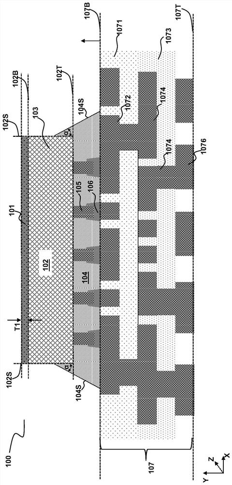
[0011] figure 1 A partial longitudinal (Z-axis direction) cross-sectional view of the flip-chip packaging unit 100 according to an embodiment of the present disclosure is illustrated. figure 1 It can be regarded as a cross-sectional view of the flip-chip packaging unit 100 on the X-Y plane in a vertical coordinate system defined by mutually perpendicular X-axis, Y-axis and Z-axis. Such as figure 1 As an example, the flip-chip packaging unit 100 may include at least one integrated circuit chip 102 packaged therein...


PUM

PropertyMeasurementUnit
Thermal conductivityaaaaaaaaaa
Thicknessaaaaaaaaaa

Abstract

The invention provides a flip chip packaging unit and a packaging method for manufacturing the flip chip packaging unit. The flip chip package unit may include an integrated circuit wafer having a wafer first surface on which a plurality of metal posts are fabricated and a wafer second surface opposite to the wafer first surface; a winding substrate which is provided with a substrate first surface and a substrate second surface opposite to the substrate first surface, wherein the wafer first surface of the integrated circuit wafer faces the substrate second surface and is welded on the winding substrate; an underfill material for filling a gap between the wafer first surface of the integrated circuit wafer and the substrate second surface; and a back surface protection film which is directly adhered to the second surface of the integrated circuit wafer, comprises one or more layers of adhesive films, can be well adhered to the back surface of the wafer, is not liable to deform and fall off after being subjected to UV illumination curing, and simultaneously meets the requirements of wafer back surface protection and wafer heat dissipation.

Description

technical field [0001] Embodiments of the present disclosure relate to integrated circuits, and in particular, to packaging structures and packaging methods for flip chips. Background technique [0002] Flip-chip packaging of chips with integrated circuits is a type of integrated circuit packaging. For integrated circuit chips that need to handle higher power, heat dissipation performance is a design index that needs to be considered. At present, when the integrated circuit chip is flip-chip packaged, it is used to wrap the chip with plastic packaging material and then remove the plastic packaging material on the back of the chip to expose the back of the chip to improve the heat dissipation effect. However, the back of the chip is exposed during storage or transportation. Increased risk of damage. Contents of the invention [0003] One aspect of the present disclosure provides an integrated circuit chip (IC) packaging structure, which may include: an integrated circuit ...

Claims


Application Information

Patent Timeline
IPC IPC(8): H01L23/31H01L23/373H01L21/56H01L21/78
CPCH01L23/3121H01L23/373H01L21/563H01L21/78H01L21/561H01L21/568H01L23/564H01L23/3171H01L24/32H01L24/16H01L2224/73204H01L2224/92125H01L2224/32225H01L2224/16227H01L2224/97H01L24/97H01L2224/94H01L21/6836H01L2221/68327H01L2221/68381H01L2224/83104H01L2224/32058H01L2224/32105H01L2224/32106H01L2224/32013H01L24/13H01L24/94H01L24/83H01L24/92H01L2224/95H01L24/81H01L2224/81801H01L2224/133H01L2224/13294H01L2224/13147H01L2224/11H01L2924/00012H01L2224/81H01L2224/83H01L2924/00014H01L2924/014H01L23/293H01L23/3164H01L24/29H01L24/73H01L2224/16225H01L2224/2919H01L2224/32057
Inventor 蒲应江蒋航郭秀宏
Owner CHENGDU MONOLITHIC POWER SYST
Features
  • R&D
  • Intellectual Property
  • Life Sciences
  • Materials
  • Tech Scout
  • Unparalleled Data Quality
  • Higher Quality Content
  • 60% Fewer Hallucinations
Learn More