Plasma processing device and heating device and working method thereof

A technology of heating device and processing device, which is applied to discharge tubes, electrical components, circuits, etc., to achieve the effect of improving the S2S distribution problem and the problem of uneven temperature

Pending Publication Date: 2021-12-03
ADVANCED MICRO FAB EQUIP INC CHINA
View PDF25 Cites 0 Cited by
  • Summary
  • Abstract
  • Description
  • Claims
  • Application Information

AI Technical Summary

Problems solved by technology

[0007] Therefore, in general, in the face of a certain asymmetric distribution inside the cavity of the plasma etching system itself and the S2S distribution caused by the previous process, it is difficult for the traditional heating device to ensure the symmetrical distribution of critical dimensions.

Method used


Image

  • Plasma processing device and heating device and working method thereof
  • Plasma processing device and heating device and working method thereof
  • Plasma processing device and heating device and working method thereof

Examples


Embodiment 1

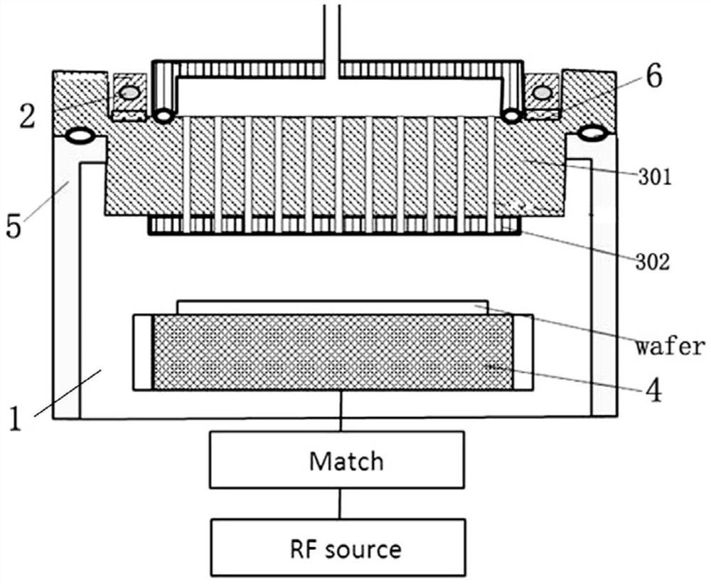
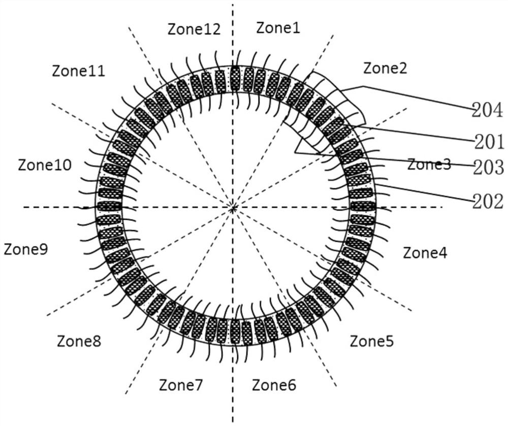
[0045] The heating device 2 includes several heating resistors 201 , a common heating source P0 and several controllers P. Among them, several heating resistors 201 are scattered and arranged in a circular ring, and the circular ring includes several zones along its circumference, which realizes the uniformity of heating provided by the heating resistors 201 and ensures the heating power received by each Zone. same;

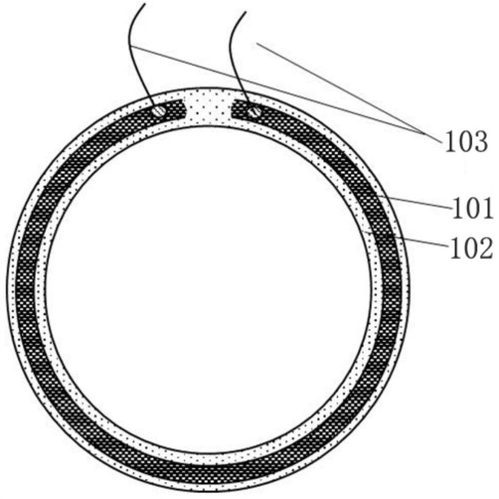
[0046] In Embodiment 1 of the present invention, the heating device 2 is discretely arranged as a plurality of surrounding heating resistors 201, which are evenly divided into several Zones, compared with the uneven heat generated at the inner and outer terminals 103 at the opening of the traditional heating resistor 101 This ensures that there is no longer a special cold spot (at the inner and outer terminals 103 at the opening of the traditional heating resistor 101) on the circumferential distribution of the heating resistor 201 of the heating device 2, and im...

Embodiment 2

[0063] The heating device 2 includes several heating resistors 201, a common heating source U0 and several controllers S. Among them, several heating resistors 201 are scattered and arranged in a circular ring, and the circular ring includes several zones along its circumference, which realizes the uniformity of heating provided by the heating resistors 201 and ensures the heating power received by each Zone. same;

[0064] In Embodiment 2 of the present invention, the heating device 2 is discretely arranged as a plurality of surrounding heating resistors 201, and is evenly divided into several Zones, compared with the uneven heat generated at the inner and outer terminals 103 at the opening of the traditional heating resistor 101 This ensures that there is no longer a special cold spot (at the inner and outer terminals 103 at the opening of the traditional heating resistor 101) on the circumferential distribution of the heating resistor 201 of the heating device 2, and improv...


PUM


Abstract

The invention discloses a heating device for a plasma processing device. The plasma processing device comprises an upper electrode, the heating device is used for heating the upper electrode, and the heating device comprises a plurality of heating resistors and a common heating source; the plurality of heating resistors are arranged in a scattering manner and surround to form a circular ring, and the circular ring comprises a plurality of areas in the circumferential direction; and the common heating source is connected with the heating resistors of all the areas and used for controlling the temperature of the heating resistors of all the areas. According to the invention, the problem that the critical dimension range and the symmetric distribution are limited in the etching process of a traditional small-critical-dimension wafer is solved, and the heating device capable of adjusting the temperature of the region is designed to adjust the region with non-uniform critical dimensions, so that the symmetric distribution of the critical dimensions is ensured, and the stability and controllability of transistor production are improved.

Description

technical field [0001] The invention relates to the technical field of integrated circuits, in particular to a plasma processing device, a heating device and a working method thereof. Background technique [0002] In the integrated circuit manufacturing industry, the critical dimension (Critical Dimension, CD) of transistors continues to shrink, and the density continues to increase. For the step of plasma etching, the critical dimension CD of the etched pattern becomes smaller and smaller. For etching equipment manufacturers, it is necessary to ensure the uniform distribution of wafer etching. If the uniform distribution of the wafer (wafer) is difficult to control during the etching process, it is easy to see the asymmetric (Side to Side, S2S) distribution on the final CD map, that is, the CD is on the same radius A certain direction (such as the 9 o'clock direction) performed significantly above or below the average. [0003] During the etch process of wafers with smal...

Claims


Application Information

Patent Timeline
Patent Type & Authority Applications(China)
IPC IPC(8): H01J37/32
CPCH01J37/32522H01J37/32568H01J2237/3345
Inventor 黄振华秦阿宾
Owner ADVANCED MICRO FAB EQUIP INC CHINA
Why Eureka
Try Eureka