SSD based on HBM cache

A solid-state disk and cache technology, applied in the direction of memory system, memory address/allocation/relocation, instrument, etc., can solve the problem of not greatly improving SSD data access capability, reducing SSD performance degradation, and unable to reduce read and write time delay

Pending Publication Date: 2021-12-07
SHANDONG SINOCHIP SEMICON
View PDF0 Cites 1 Cited by
  • Summary
  • Abstract
  • Description
  • Claims
  • Application Information

AI Technical Summary

Problems solved by technology

However, this method is also a solution to reduce write amplification and garbage collection, which can only reduce the ...

Method used


Image

  • SSD based on HBM cache
  • SSD based on HBM cache

Examples


Embodiment 1

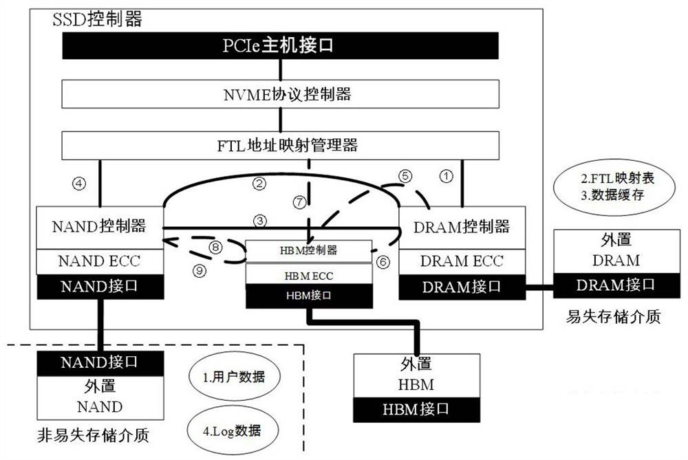
[0038] The SSD solid-state disk based on the HBM and DRAM hybrid cache described in Embodiment 1 uses DRAM to process FTL address mapping table information, uses large-capacity, high-speed HBM cache to process application data, and performs data garbage collection operations during continuous writing. Reduce the reading and writing pressure of DRAM, ensure the update efficiency of FTL address data, improve the processing efficiency of application data at the same time, speed up the data relocation speed in the garbage collection process, and reduce the impact of write amplification on the performance of the entire disk. Compared with traditional SSD solid state disk has a more powerful ability to receive data. Taking 8TB SSD as an example, the required cache capacity for FTL is 8GB, and a DDR cache chip is used as the storage space for its FTL address mapping table; at the same time, a large-capacity HBM2E cache (capacity 16GB~64GB) is configured, and one HBM2E chip is enough ...

Embodiment 2

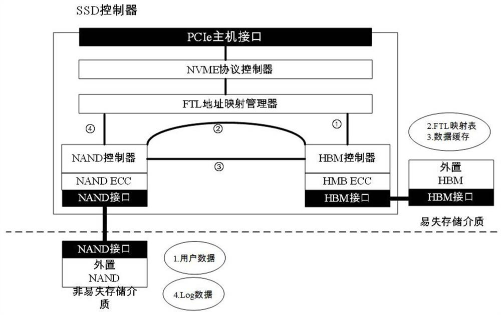
[0039] The SSD solid state disk based on the HBM cache described in Embodiment 2 has a stronger ability to receive data than ordinary SSD solid state disks. Taking an 8TB SSD as an example, the required cache capacity for FTL is 8GB. With a DDR4.0 cache chip, 4 DRAM chips need to be pasted; if HBM2E with a single-chip maximum capacity of 16GB is used, 1 HBM2E chip can meet the capacity And performance requirements, when increased to 4 slices, the total cache capacity reaches 64GB, and the excess cache capacity can bear the data writing or reading "margin" of more than 8s ((64GB-8GB) / 7GB / s = 8s) , which greatly improves the data receiving capability of the SSD solid state disk, and can shield the read and write delay of the NAND flash memory.

[0040] Example 1

[0041] This embodiment discloses an SSD solid state disk based on HBM and DRAM hybrid cache, such as figure 1 As shown, including SSD controller, DRAM cache controller, HBM cache controller and NAND controller, D...


PUM


Abstract

The invention relates to an SSD based on an HBM cache, and the SSD comprises an SSD based on the HBM and DRAM hybrid cache and an SSD based on the HBM cache; the SSD based on the HBM and DRAM hybrid cache mixedly uses the HBM and the DRAM as the cache, the DRAM stores an FTL (File Transfer Layer) mapping table, and the HBM provides a cache function. According to the SSD based on the HBM cache, the HBM is used for replacing a DRAM, and the HBM has the functions of caching data and storing an FTL mapping table. According to the method, the constant read-write bandwidth is ensured in the process of processing write amplification and garbage collection, the read-write time delay is reduced, and the high-concurrency multi-channel video data access efficiency is ensured to a greater extent.

Description

technical field [0001] The invention relates to the field of solid-state storage, in particular to an HBM cache-based SSD solid-state disk. Background technique [0002] The main components of SSD solid state disk include main control chip, flash memory particles, cache chip, PCB, etc. Among them, the main control chip controls and manages the space of all flash memory particles, and determines the specific distribution position of data on the flash memory particles. Flash memory particles provide actual storage space for storing actual application data. The PCB is the base of the SSD, on which all chips and related electronic components are soldered, and is the basis of the SSD. The cache chip is a special existence in the SSD solid state disk. Its main function is to store the FTL address mapping table, which indicates the correspondence (mapping) relationship between the physical address of the unit space in the flash memory particle and the logical address of the file ...

Claims


Application Information

Patent Timeline
IPC IPC(8): G06F13/16G06F13/42G06F12/02
CPCG06F13/1668G06F13/4282G06F12/0246G06F2213/0026
Inventor 李瑞东郭鹏
Owner SHANDONG SINOCHIP SEMICON
Why Eureka
Try Eureka