PCB micro-etching process of micro circuit and circuit board

A micro-etching, circuit board technology, applied in printed circuits, printed circuit manufacturing, printed circuit secondary processing, etc., can solve the problems of low production efficiency and low yield of circuit boards, and achieve high yield and production The effect of rate reduction and etch time extension

Pending Publication Date: 2021-12-07
江西景旺精密电路有限公司
View PDF4 Cites 2 Cited by
  • Summary
  • Abstract
  • Description
  • Claims
  • Application Information

AI Technical Summary

Problems solved by technology

[0005] The object of the present invention is to provide a PCB micro-etching process and circuit board for micro-circuits, aiming to solve the problems of low production efficiency and low yield of circuit boards for micro-circuits

Method used


Image

  • PCB micro-etching process of micro circuit and circuit board

Examples


Embodiment Construction

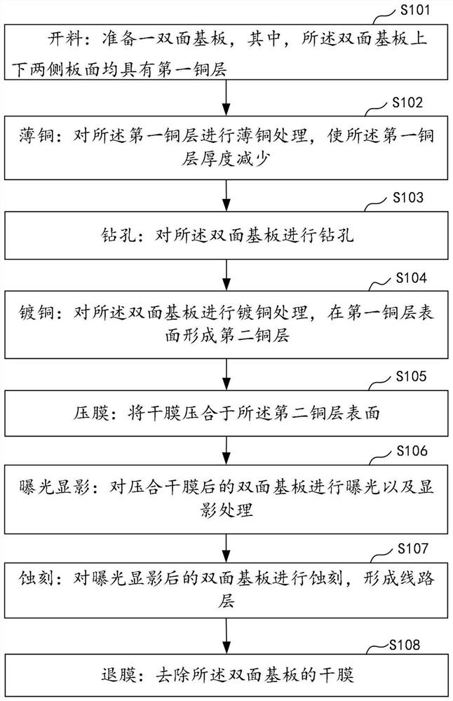
[0042] The following will clearly and completely describe the technical solutions in the embodiments of the present invention with reference to the accompanying drawings in the embodiments of the present invention. Obviously, the described embodiments are some of the embodiments of the present invention, but not all of them. Based on the embodiments of the present invention, all other embodiments obtained by persons of ordinary skill in the art without making creative efforts belong to the protection scope of the present invention.

[0043] It should be understood that when used in this specification and the appended claims, the terms "comprising" and "comprises" indicate the presence of described features, integers, steps, operations, elements and / or components, but do not exclude one or Presence or addition of multiple other features, integers, steps, operations, elements, components and / or collections thereof.

[0044] It should also be understood that the terminology used ...


PUM

PropertyMeasurementUnit
thicknessaaaaaaaaaa

Abstract

The embodiment of the invention discloses a PCB micro-etching process of a micro circuit and a circuit board. The PCB micro-etching process comprises the following steps: cutting: preparing a double-sided substrate, and the upper and lower side plate surfaces of the double-sided substrate being respectively provided with a first copper layer; copper thinning: carrying out copper thinning treatment on the first copper layer to reduce the thickness of the first copper layer; drilling: specifically, performing drilling on the double-face substrate; copper plating: performing copper plating treatment on the double-sided substrate, and forming a second copper layer on the surface of the first copper layer; film pressing: pressing a dry film on the surface of the second copper layer; exposing, developing, etching and stripping the film. According to the embodiment of the invention, the first copper layer is subjected to copper thinning treatment, so that the thickness of the first copper layer is reduced to be within the preset thickness range, the etching rate of the circuit board is reduced, namely, the etching time of the circuit board is prolonged, the circuit layer of the circuit board is accurately controlled, and the yield and the production efficiency of the circuit board are effectively improved.

Description

technical field [0001] The invention relates to the field of printed circuit boards, in particular to a PCB micro-etching process for fine lines and a circuit board. Background technique [0002] At present, with the rapid development of science and technology, the electronics industry is at the forefront of technological development. PCB (printed circuit board) products in electronics are increasingly tending to be integrated and miniaturized. Among them, the micro-circuit 40 / 40μm will become a future trend. [0003] At present, factories producing circuit boards, in the prior art, often use etching potions to etch the exposed and developed circuit boards, so as to obtain the circuits of the circuit boards. However, since the etching potions are copper chloride systems, they are acidic. It is easy to control the etching rate of the circuit board. If the etching rate is too fast, the etching of the circuit will be incomplete. Otherwise, the etching will be over-etched, caus...

Claims


Application Information

Patent Timeline
Patent Type & Authority Applications(China)
IPC IPC(8): H05K3/00H05K3/06H05K3/24
CPCH05K3/0017H05K3/0047H05K3/06H05K3/244
Inventor 王均臣张伦亮王春雪王亮朱爱军
Owner 江西景旺精密电路有限公司
Why Eureka
Try Eureka