Schottky diode with multi-protection ring structure

A technology of Schottky diodes and guard rings, applied in the direction of electrical components, circuits, semiconductor devices, etc., can solve problems such as collapse and limited potential buffering capacity, and achieve the effect of preventing premature collapse and preventing the accumulation of surface charges

Pending Publication Date: 2021-12-17
TAIWAN SEMICON MFG CO LTD
View PDF0 Cites 0 Cited by
  • Summary
  • Abstract
  • Description
  • Claims
  • Application Information

AI Technical Summary

Problems solved by technology

[0008] As mentioned above, the existing trench Schottky diode PA100 mainly extends the first metal layer PA5 and the second metal layer PA7 to the termination area to increase the reverse bias voltage, and a guard ring structure PA33 is provided on the epitaxial layer PA3 To disperse the potential, but due to the limited potential buffering capacity of the guard ring structure PA33, the charge of the trench Schottky diode PA100 is still easy to concentrate in the termination area of ​​the edge and prone to premature collapse

Method used


Image

  • Schottky diode with multi-protection ring structure
  • Schottky diode with multi-protection ring structure
  • Schottky diode with multi-protection ring structure

Examples


Embodiment Construction

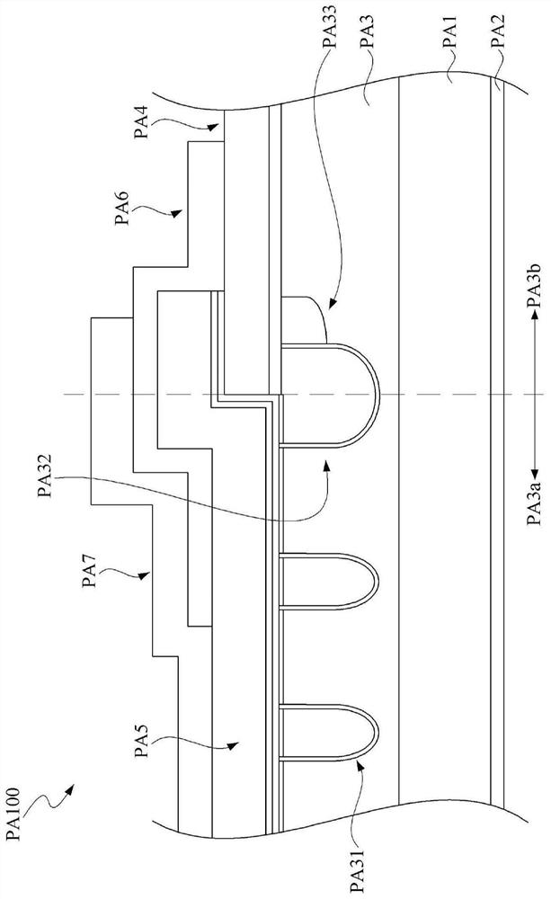
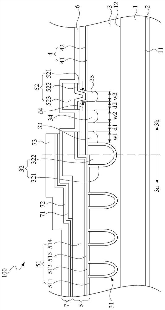
[0080] See figure 2 , figure 2 It is a preferred embodiment of the present invention having a cross-sectional view of the multiple guard ring structure according Schottky diode is provided. As shown, the guard ring structure having a plurality of Schottky diode 100 includes a semiconductor substrate 1, a back metal layer 2, an epitaxial layer 3, dielectric layer 4, a first metal layer 5, a blunt layer 6 and a second metal layer 7.

[0081] The semiconductor substrate 1 has a back surface opposite a front surface 11 and 12, and the semiconductor substrate 1 is a heavily doped N-type silicon layer. A back metal layer 2 is formed on the back surface 11 of the semiconductor substrate 1, and the metal back layer 2 composition comprises titanium, nickel, silver, or combinations thereof. Epitaxial layer 3 is formed on the front surface 121 of semiconductor base layer, and having a cell area adjacent to a termination region 3a and 3B, the epitaxial layer 3 and a lightly doped N-type silic...


PUM


Abstract

The invention discloses a Schottky diode with a multi-protection ring structure. The Schottky diode comprises a semiconductor base layer, a back metal layer, an epitaxial layer, a dielectric layer, a first metal layer, a passivation layer and a second metal layer, wherein the epitaxial layer is stacked on the semiconductor base layer, and comprises a terminal groove structure, a first ion implantation protection ring, a second ion implantation protection ring and a third ion implantation protection ring. The dielectric layer is stacked on the epitaxial layer in a termination region. The first metal layer is stacked on the terminal groove structure and the dielectric layer and is provided with a groove. The passivation layer is stacked on the first metal layer and the dielectric layer. The second metal layer is stacked on the first metal layer and the passivation layer. The widths of the first ion implantation protection ring, the second ion implantation protection ring and the third ion implantation protection ring are sequentially decreased, so that voltage is effectively distributed step by step.

Description

Technical field [0001] The present invention relates to a Schottky diode, particularly to a guard ring structure having a plurality of Schottky diodes. Background technique [0002] In general, the ideal rectifier should have a low smooth pressure drop, high reverse crash voltage and zero-drain current, in which a low smooth pressure has a low smooth pressure due to a thintest diode with a metal-semiconductor tape as a baptist barrier. The characteristics of the high-speed switching are therefore widely used in the power rectifier element, but the wedgel diode still has a shortcoming of the reverse bias and the reverse leakage current of the reverse leakage current, thereby restricting the application of the Xiaoteki diode. [0003] In contracted, the Diki diode is mainly divided into a traditional flat weddtky diode (Trench Schottky). The flat wedgel diode mainly forms a stacked structure to a stack of a layer of semiconductor and metal, often requires a selection between the di...

Claims


Application Information

Patent Timeline
Patent Type & Authority Applications(China)
IPC IPC(8): H01L29/06H01L29/872
CPCH01L29/872H01L29/0684H01L29/0696H01L29/0615H01L29/0619H01L29/0623
Inventor 蔡宜龙赛德·萨瓦·伊玛目庄曜维董铭楼
Owner TAIWAN SEMICON MFG CO LTD
Why Eureka
Try Eureka