A method for preparing a sample for transmission electron microscopy

An electron microscope and sample technology, applied in the preparation of test samples, material analysis using radiation, material analysis using wave/particle radiation, etc., can solve problems such as damage, failure to show contrast of protective layer, and damaged structure

Pending Publication Date: 2021-12-21
INTERUNIVERSITAIR MICRO ELECTRONICS CENT (IMEC VZW)
View PDF0 Cites 0 Cited by
  • Summary
  • Abstract
  • Description
  • Claims
  • Application Information

AI Technical Summary

Problems solved by technology

However, samples with a polymer top surface (such as including a patterned polymer photoresist layer) are easily damaged by any of the above methods, or these samples do not exhibit enough contrast with the protective layer to be detected during transmission electron microscope observation. be distinguished
In the case of fragile structures such as polymer resist lines or porous silicon structures, the deposition of additional contrast layers by sputtering techniques is not an option because sputtering techniques will destroy the structure

Method used


Image

  • A method for preparing a sample for transmission electron microscopy
  • A method for preparing a sample for transmission electron microscopy
  • A method for preparing a sample for transmission electron microscopy

Examples


Embodiment Construction

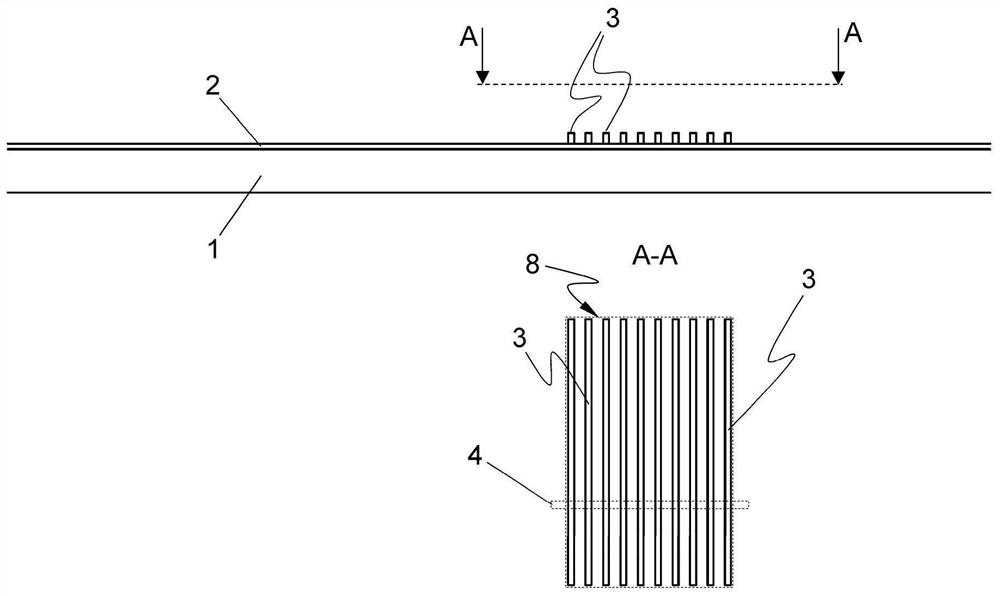
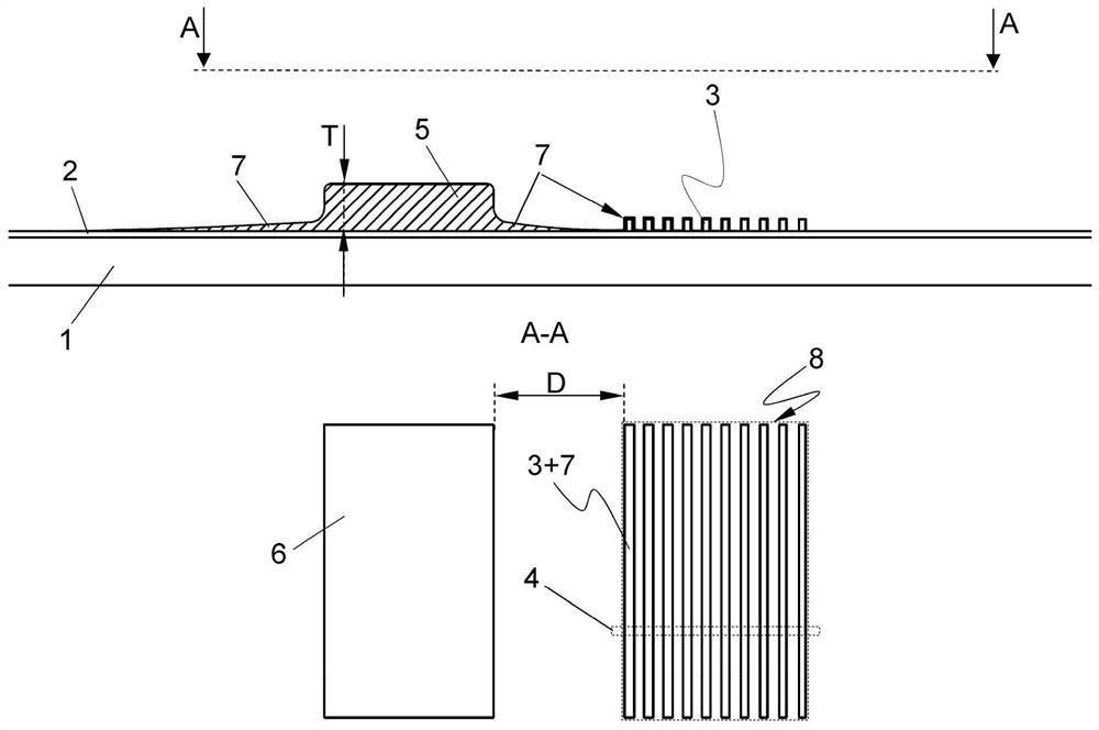
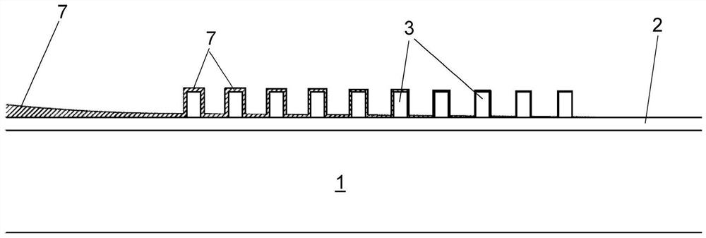
[0022] A preferred embodiment of the invention will be described for the case of a set of parallel polymeric resist lines. Said materials and processes known per se are mentioned by way of example only and are not intended to limit the scope of the invention. figure 1 Shown is a substrate 1 , which may be a glass substrate, which has a silicon layer 2 on its surface. On the Si layer is a patterned area 8 comprising an array of parallel polymer resist lines 3, produced by a lithographic patterning technique per se known in the art . The pitches of the line arrays are of the same order of magnitude. The goal is to obtain TEM samples that allow verification of these dimensions. To do this, a protective spin-on-carbon (SoC) layer is deposited on the resist line 3 and either side of the lamella oriented in a direction perpendicular to the line 3 is milled away in a focused ion beam (FIB) tool. materials to generate substrate TEM samples. The profile of sample 4 is at figure 1...


PUM


Abstract

A substrate is provided comprising on its surface a patterned area defined by a given topography. The substrate is to be processed for obtaining a TEM sample in the form of a slice of the substrate. According to the method of the invention, a conformal layer of contrasting material is deposited on the topography, by depositing a layer of the contrasting material on a local target area of the substrate, spaced apart from the patterned area. The material is deposited by Electron Beam Induced Deposition (EBID). The deposition parameters, the thickness of the layer deposited in the target area, and the distance of said target area to the patterned area, are such that a conformal layer of the contrasting material is formed on the topography of the patterned area. This is followed by the deposition of the protective layer, which does not damage the topography in the patterned area, as it is protected by the conformal layer. The TEM sample is prepared in a manner known in the prior art, for example by FIB. The conformal contrasting layer provides a good contrast with the protective layer, thereby allowing a high quality TEM analysis.

Description

technical field [0001] The present invention relates to the field of transmission electron microscopy (TEM), and more particularly to methods for preparing TEM samples to visualize nanoscale structures such as are produced in semiconductor processing. Background technique [0002] Transmission electron microscopes are widely used in the semiconductor industry to observe the finest details of transistor and memory structures down to the atomic level. One of the difficult steps is sample preparation for TEM. This is done in a focused ion beam milling (FIB) tool, whereby flakes of the order of tens of nanometers are removed from the samples under study. Sample slices need to be thin enough to show electron transparency. In order to protect the structure itself from being milled during the preparation of the lamella, masks and protective layers are required. The protective layer can be applied by various methods: spin coating, physical vapor deposition, chemical vapor deposit...

Claims


Application Information

Patent Timeline
Patent Type & Authority Applications(China)
IPC IPC(8): G01N23/2202G01N1/28G01N23/04G01N23/22
CPCG01N23/2202G01N1/28G01N23/04G01N23/22C23C16/487H01J37/3053H01J37/3178G01N1/2813C23C16/06C23C16/045G01N1/32H01J37/261H01J2237/262H01J2237/2802
Inventor E·范科耶N·博斯曼P·卡罗兰
Owner INTERUNIVERSITAIR MICRO ELECTRONICS CENT (IMEC VZW)
Why Eureka
Try Eureka