Method for improving modulation bandwidth of micro LED by using atomic layer deposition technology

A technology of atomic layer deposition and bandwidth modulation, which is applied in the field of optical communication, can solve the problems of Mini-LED/Micro-LED heat generation, limit optical communication rate and distance, and hinder the popularization of optical communication, so as to improve carrier life, Effect of improving luminous intensity, good innovation and feasibility

Pending Publication Date: 2021-12-28
XIAMEN UNIV
View PDF0 Cites 0 Cited by
  • Summary
  • Abstract
  • Description
  • Claims
  • Application Information

AI Technical Summary

Problems solved by technology

[0008] The commonly used light source in the VLC system is a C-plane micro light-emitting diode based on InGaN quantum wells, but the current modulation bandwidth of the light source is inherently limited by the carrier recombination rate, but with the reduction of the chip size, the current density injection efficiency of the chip can be improved. Significantly improved, and the carrier lifetime is significantly shortened compared with ordinary LEDs. Therefore, small-sized LED chips have broad application prospects in the field of optical communications. However, the current preparation method of small-sized Ш-nitride LEDs is mainly through dry etching technology. , this method will inevitably cause damage to the side wall of the chip, which will lead to aggravated heat generation and performance degradation of Mini-LED / Micro-LED, especially the increase in carrier life and weakened luminous intensity, thereby limiting the rate and speed of optical communication. distance, hindering the popularization of optical communication

Method used


Image

  • Method for improving modulation bandwidth of micro LED by using atomic layer deposition technology
  • Method for improving modulation bandwidth of micro LED by using atomic layer deposition technology
  • Method for improving modulation bandwidth of micro LED by using atomic layer deposition technology

Examples


Embodiment Construction

[0028] In order to make the object, technical solution and advantages of the present invention more clear, the following embodiments will further illustrate the present invention in conjunction with the accompanying drawings. It should be understood that the specific embodiments described here are only examples of specific implementation examples of the present invention, and are only used to explain the present invention, not to limit the present invention.

[0029] The following embodiments will further illustrate the present invention in conjunction with the accompanying drawings.

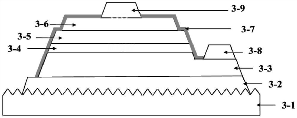
[0030] see figure 1 , describing the ALD sidewall repair process of Mini-LED / Micro-LED and the information exchange process of the system when the device is used as a light source for an optical communication system.

[0031] The Ethernet signal 1 is transmitted to the driver module 2, and the driver module 2 couples the input signal and the DC signal, and loads the coupled signal to both ends ...


PUM

PropertyMeasurementUnit
thicknessaaaaaaaaaa

Abstract

The invention discloses a method for improving the modulation bandwidth of a micro LED by using an atomic layer deposition technology, and relates to the technical field of optical communication. According to the method for improving the modulation bandwidth of the micro LED by using the atomic layer deposition technology an ALD with a certain thickness is deposited on the side wall of a Mini-LED/Micro-LED to reduce the service life of a current carrier so as to obtain a high modulation bandwidth, and finally the purpose of improving the VLC communication rate is achieved; the purposes of repairing side wall damage, reducing the service life of a current carrier and further improving the modulation bandwidth and the luminous intensity of the device are achieved, and the modulation bandwidth of Mini-LED/Micro-LED is improved by reducing the service life of the current carrier, so the communication rate of the system is further improved; and the luminous intensity is improved by improving the service life of the current carrier, so that the communication distance of the system is further increased. And a positive promotion effect is achieved for promoting the universal application of the communication mode with rich spectrum and high confidentiality in the future.

Description

technical field [0001] The invention relates to the technical field of optical communication, in particular to a method for improving the modulation bandwidth of micro-LEDs by using atomic layer deposition technology. Background technique [0002] Optical communication technology refers to the communication method that directly transmits optical signals in the air by using light in the visible light band as an information carrier, without using optical fiber and other wired channel transmission media. Mini-LED / Micro-LED optical communication is based on the fast switching speed of Mini-LED / Micro-LED. A high-speed light wave signal is used to modulate and transmit information, and then a communication technology that receives the optical signal through a photoelectric converter such as APD and restores the original information from the optical signal. Regardless of the optical communication system used in any scenario, it is composed of input and processing circuits, drive m...

Claims


Application Information

Patent Timeline
Patent Type & Authority Applications(China)
IPC IPC(8): H01L33/44C23C16/40C23C16/455H04B10/116
CPCH01L33/44C23C16/403C23C16/45525H04B10/116H01L2933/0025
Inventor 吴挺竹林万胜潘建华卢霆威郭伟杰林岳陈国龙郭自泉吕毅军陈忠
Owner XIAMEN UNIV
Why Eureka
Try Eureka