Terahertz modulator based on mode coupling

A mode-coupling and terahertz technology, applied in instruments, nonlinear optics, optics, etc., can solve problems such as limited modulation depth, low device sensitivity, and low Q value, and achieve easy packaging, mature technology, and good frequency selection Effects of Characteristics and Sensitivity

Inactive Publication Date: 2016-06-15
UNIV OF ELECTRONICS SCI & TECH OF CHINA
View PDF5 Cites 16 Cited by
  • Summary
  • Abstract
  • Description
  • Claims
  • Application Information

AI Technical Summary

Problems solved by technology

First of all, the semiconductor material in the composite structure currently used at home and abroad is usually a bulk material, which will introduce large parasitic parameters, which is not conducive to the improvement of the modulation rate; secondly, the artificial microstructure in the com...

Method used


Image

  • Terahertz modulator based on mode coupling
  • Terahertz modulator based on mode coupling
  • Terahertz modulator based on mode coupling

Examples


Embodiment Construction

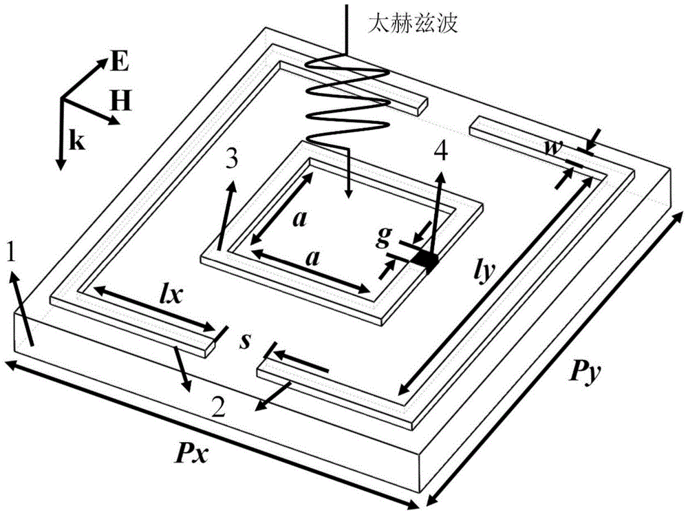
[0013] The terahertz modulator unit based on mode coupling such as figure 1 As shown, it is composed of a substrate (1), artificial microstructures (2, 3) and controllable dynamic materials (4). The artificial microstructure is composed of metal lines with a line width of w obtained after photolithography of the metal film on the substrate, and the thickness is usually 200-500 nm. The metal pattern is divided into two parts, namely, a bright mode resonant unit (2) and a dark mode resonant unit (3). The bright mode resonant unit is a symmetrically placed U-shaped dipole oscillation structure located on the periphery of the pattern, and it has a strong resonance ability for incident electromagnetic waves. The length of the main arm of the U-shaped structure is ly, the length of the auxiliary arm is lx, and the distance between the two U-shaped structures is s. The dark mode resonant unit is a square open resonant ring with a side length a and an opening width g located inside th...


PUM


Abstract

The invention relates to a terahertz modulator based on mode coupling and belongs to the technical field of electromagnetic functional devices. The terahertz modulator is formed by a substrate, a mode coupling artificial microstructure and a controllable dynamic semiconductor material. The mode coupling artificial microstructure comprises a bright mode resonance unit and a dark mode resonance unit. The dark mode resonance unit is located at the center of the bright mode resonance unit, and the two resonance units are subject to mode coupling to form an electromagnetic induction transmission window. The dynamic semiconductor material is located at the position of an opening of the dark mode resonance unit; under additional excitation, the dark mode working mode can be changed so that mode coupling between a bright mode and a dark mode is affected, and finally the tunable electromagnetic induction transmission window is obtained. The bright mode resonance unit and the dark mode resonance unit have the same resonance frequency point, so that very good coupling can be achieved between the bright mode and the dark mode, and the modulation bandwidth has a high Q value and large modulation depth. The terahertz modulator is processed in a micro machining mode, and a preparation process is mature and reliable. An obtained device is flexible and convenient to use and has very high potential application value in the field of terahertz wireless communication.

Description

Technical field [0001] The invention belongs to the technical field of electromagnetic functional devices, as well as the field of communication devices including modulators, filters, photoconductive switches, etc. Background technique [0002] As the core device of the terahertz wireless communication system, the terahertz modulator has become a research hotspot in the field of terahertz dynamic devices in recent years. The terahertz modulator can be constructed by combining artificial microstructures with semiconductor materials, usually by photoetching a layer of artificial microstructured metal film on a semiconductor material substrate, and realizing dynamics of terahertz waves under temperature, light and voltage excitation conditions control. This scheme makes full use of the frequency response characteristics of artificial microstructures and the dynamic characteristics of semiconductor materials, and is a composite structure scheme. Although the terahertz modulator pre...

Claims


Application Information

Patent Timeline
IPC IPC(8): G02F1/01
CPCG02F1/0102
Inventor 张雅鑫乔绅赵运成梁士雄杨梓强
Owner UNIV OF ELECTRONICS SCI & TECH OF CHINA
Why Eureka
Try Eureka