Photoelastic method based on single-pixel imaging

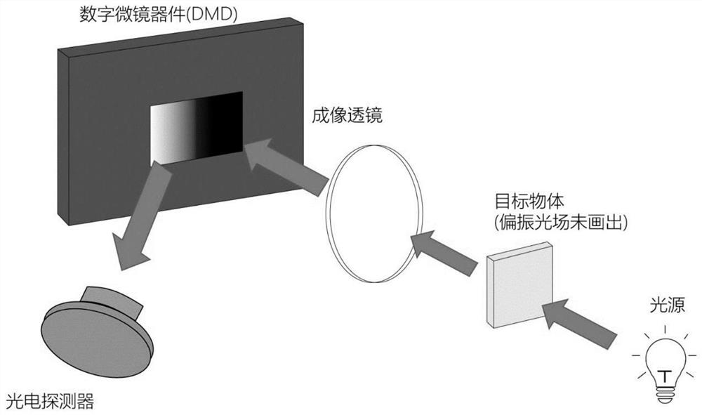
A single-pixel, photoelastic technology, applied in the field of optical imaging, can solve the problems of CCD or CMOS cameras that are difficult to manufacture, complex lens groups, and expensive, and achieve short response time, simplified optical design, and low manufacturing costs.

Active Publication Date: 2021-12-28
HEFEI UNIV OF TECH
View PDF2 Cites 0 Cited by
  • Summary
  • Abstract
  • Description
  • Claims
  • Application Information

AI Technical Summary

Problems solved by technology

[0003] The CCD or CMOS camera used in the traditional photoelastic method has a complex structure, high cost and high cost, and it is difficult to manufacture or even unobtainable CCD or CMOS camera suitable for some special wave bands (infrared, ultraviolet, etc.), and the use of the camera also requires a relatively complicated lens group, which also increases the cost of

Method used


Image

  • Photoelastic method based on single-pixel imaging
  • Photoelastic method based on single-pixel imaging
  • Photoelastic method based on single-pixel imaging

Examples


Embodiment Construction

[0038] In order to make the purpose, technical solutions and advantages of the embodiments of the present invention clearer, the technical solutions in the embodiments of the present invention will be clearly and completely described below in conjunction with the drawings in the embodiments of the present invention. Obviously, the described embodiments It is a part of embodiments of the present invention, but not all embodiments.

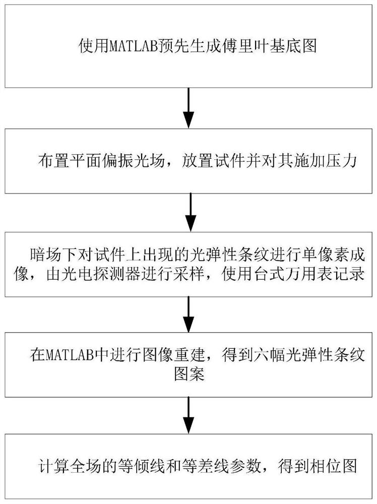
[0039] Before introducing the embodiments of the present invention, the technical idea of ​​the present invention will be described in combination with the traditional photoelastic method and the Fourier single-pixel imaging method:

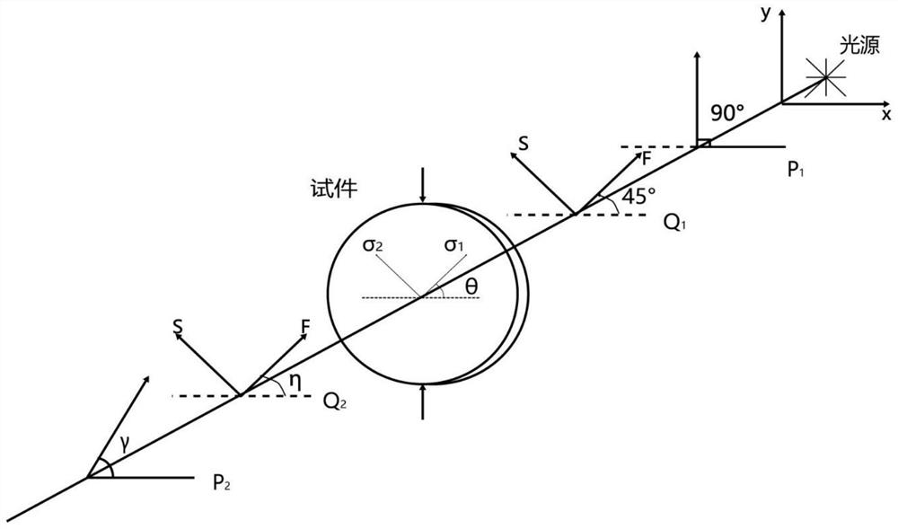
[0040] 1. Principle of photoelasticity method

[0041] The key to the stress analysis of the photoelastic method is to obtain the phase diagram of the isocline and contour line. The six-step phase shift method is one of the most commonly used methods in the image processing of the photoelastic method. The settings are ...


PUM


Abstract

The invention relates to a photoelastic method based on single-pixel imaging, the method is based on a single-pixel imaging light path of a DMD (Digital Micromirror Device), and comprises the following steps of: pre-generating a Fourier base map by using MATLAB (Matrix Laboratory); arranging a plane polarized light field, placing a test piece and applying pressure to the test piece; performing single-pixel imaging on photoelastic stripes appearing on the test piece in a dark field, sampling by using a photoelectric detector, and recording by using a table-type universal meter; carrying out image reconstruction in MATLAB to obtain six photoelastic stripe patterns; and calculating the isoclinal line and isochromatic line parameters of the whole field to obtain a phase diagram. According to the invention, a single-pixel imaging technology is introduced to replace a CCD camera or a CMOS camera, imaging can be carried out only by using a single-pixel detector without spatial information resolution capability, the structure is simple, an imaging system does not need a complex lens group, and the optical design can be greatly simplified. Compared with an array type detector, the single-pixel detector has the advantages of higher quantum efficiency, lower dark noise, shorter response time and the like, and the manufacturing cost is lower.

Description

technical field [0001] The invention relates to the technical field of optical imaging, in particular to a photoelastic method based on single-pixel imaging. Background technique [0002] The traditional photoelastic method uses an array of silicon-based charge-coupled devices (Charge Coupled Device, CCD) or complementary metal oxide semiconductor (Complementary Metal Oxide Semiconductor, CMOS) cameras to obtain photoelastic fringe images. [0003] The CCD or CMOS camera used in the traditional photoelastic method has a complex structure, high cost and high cost, and it is difficult to manufacture or even unobtainable CCD or CMOS camera suitable for some special wave bands (infrared, ultraviolet, etc.), and the use of the camera also requires a relatively complicated lens Group, also raised the cost. Contents of the invention [0004] The present invention proposes a photoelastic method based on single-pixel imaging. The present invention introduces a single-pixel imaging...

Claims


Application Information

Patent Timeline
Patent Type & Authority Applications(China)
IPC IPC(8): H04N5/225H04N5/232
CPCH04N23/56H04N23/55H04N23/80
Inventor 邓华夏黄晓宇高夕成管擎天马孟超钟翔
Owner HEFEI UNIV OF TECH
Why Eureka
Try Eureka