Solar cell and method for fabricating a solar cell

A technology of solar cells and dielectrics, applied in the field of solar cells

Pending Publication Date: 2021-12-31
NAT UNIV OF SINGAPORE
View PDF0 Cites 0 Cited by
  • Summary
  • Abstract
  • Description
  • Claims
  • Application Information

AI Technical Summary

Problems solved by technology

would require a large number

Method used


Image

  • Solar cell and method for fabricating a solar cell
  • Solar cell and method for fabricating a solar cell
  • Solar cell and method for fabricating a solar cell

Examples


Embodiment Construction

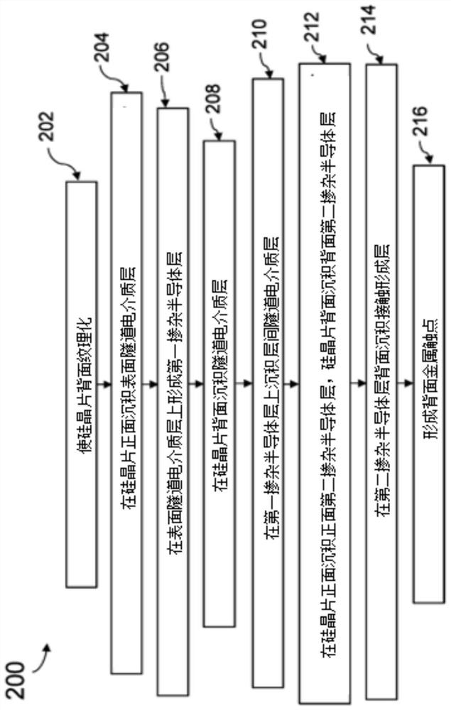
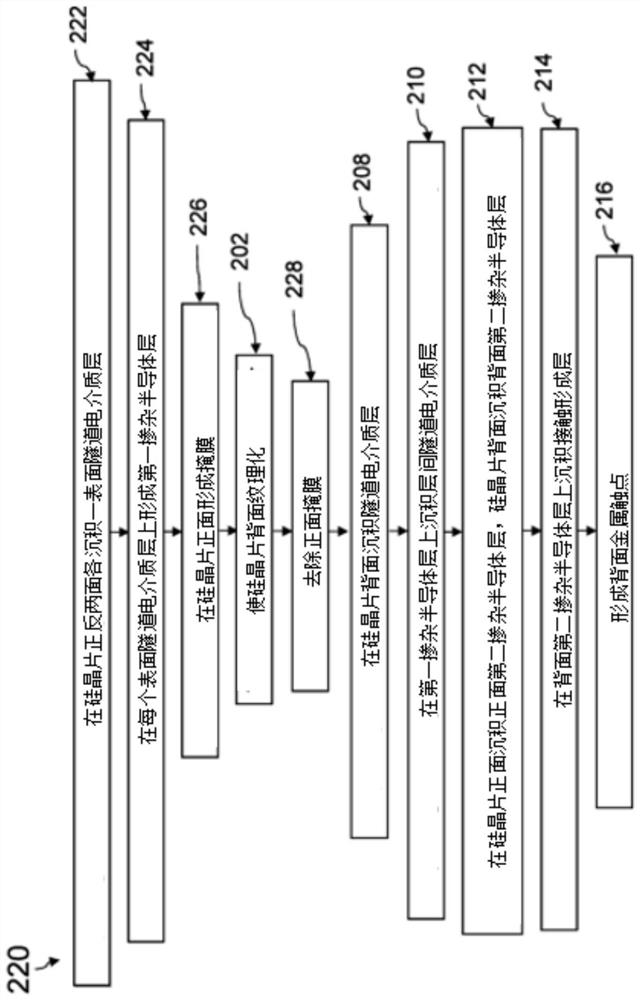
[0059] One embodiment relates to a method for manufacturing a solar cell, in particular a passivated contact solar cell with a tunnel junction.

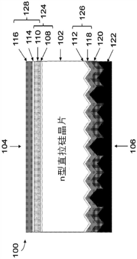
[0060] figure 1 is a structural schematic diagram of a solar cell (100) drawn according to an embodiment. The solar cell (100) can be configured as a high-efficiency silicon bottom cell for integration of tandem thin-film silicon devices, as described below Figure 13 mentioned. Different types of solar cells (100) configured as high-efficiency silicon bottom cells, Figures 11A to 11C The integration of tandem thin-film silicon devices is further discussed.

[0061] A solar cell (100) includes an n-type Czochralski (Cz) grown monocrystalline silicon wafer (102) having a front side (104) and a back side (106). Such as figure 1 As shown, the front side (104) of the silicon wafer (102) has a smooth surface, while the back side (106) of the silicon wafer (102) has a textured surface. A surface tunnel dielectric layer (108) is de...


PUM


Abstract

A solar cell is described. In an embodiment, the solar cell (100) comprises a silicon wafer having (102) a front side (104) arranged to receive incident light and a rear side (106), and a first doped semiconductor layer (110) formed on either the front side (104) or the rear side (106) of the silicon wafer (102). The solar cell (100) further comprises (i) a dielectric tunnel layer (112) deposited on one side of the silicon wafer (102) opposites to the side at which the first doped semiconductor layer (110) is formed, (ii) a front side second doped semiconductor layer (116) deposited on the front side (104) of the silicon wafer (102); and (iii) a rear side second doped semiconductor layer (118) deposited on the rear side (106) of the silicon wafer (102), the front side and the rear side second doped semiconductor layers (116), (118) each having a doping of an opposite polarity to the first doped semiconductor layer (110). The first doped semiconductor layer (110) cooperates with either the front side second doped semiconductor layer (116) or the rear side second doped semiconductor layer (118) to form a tunnel junction, and the dielectric tunnel layer (112) cooperates with either the rear side second doped semiconductor layer (118) or the front side second doped semiconductor layer (116) to form a passivated contact.

Description

technical field [0001] The invention relates to a solar cell and a method of manufacturing a solar cell, in particular a passivated contact solar cell with a tunnel junction. Background technique [0002] The photovoltaic market is currently dominated by wafer-based crystalline silicon (Si) solar cells. Under the premise of considering the Auger recombination effect, in order to achieve ultra-high efficiency (close to the theoretical limit) of 29% for silicon solar cells, passivated contacts are an attractive option. Specifically, passivating contacts reduces recombination losses at solar cell contacts, since recombination at solar cell contacts constitutes the main loss mechanism, thereby increasing the open circuit voltage and efficiency of solar cells. [0003] Currently, in order to form passivation contacts (e.g., SiO for electron extraction x / n + poly-Si or SiO for hole extraction x / p + poly-Si), usually using double-sided deposition methods, especially tube dep...

Claims


Application Information

Patent Timeline
IPC IPC(8): H01L31/06H01L31/18
CPCY02E10/50H01L31/02167H01L31/0745H01L31/078H01L31/043
Inventor 斯坦格尔罗尔夫孟思威林志鹏黄信仁林棻
Owner NAT UNIV OF SINGAPORE
Why Eureka
Try Eureka