Supercharge Your Innovation With Domain-Expert AI Agents!

Power semiconductor characteristic parameter test system and method

A technology of power semiconductors and characteristic parameters, which is applied in the direction of single semiconductor device testing, measuring electricity, measuring devices, etc., can solve the adverse effects of power electronic devices, does not target and adapt to high-voltage SiC power devices, and cannot dynamic characteristics of high-voltage SiC power devices Problems such as parameter testing, to achieve the effect of improving the accuracy of parameter testing, avoiding electromagnetic interference, and realizing high current carrying

Pending Publication Date: 2022-01-04
ELECTRIC POWER RES INST OF STATE GRID ZHEJIANG ELECTRIC POWER COMAPNY +1
View PDF0 Cites 2 Cited by
  • Summary
  • Abstract
  • Description
  • Claims
  • Application Information

AI Technical Summary

Problems solved by technology

[0008] In the current commercial market, many domestic and foreign manufacturers have introduced test system equipment for the dynamic characteristic parameters of power semiconductor devices, but most of them use traditional Si devices as test objects, and regard the dynamic characteristics of Si devices as the technical requirements of their test systems. The parasitic parameters of dynamic test equipment can only meet the test requirements of low-speed switching characteristics of traditional power devices, and are not aimed at and adapted to high-voltage SiC power devices. Therefore, the existing technology cannot perform high-precision dynamic characteristics of third-generation semiconductor high-voltage SiC power devices. Parametric testing, which in turn has an adverse impact on the promotion, application and industry development of power electronic devices in my country

Method used


Image

  • Power semiconductor characteristic parameter test system and method
  • Power semiconductor characteristic parameter test system and method
  • Power semiconductor characteristic parameter test system and method

Examples


Embodiment Construction

[0069] In order to make the object, technical solution and advantages of the present invention clearer, the present invention will be further described in detail below in conjunction with the accompanying drawings and embodiments. It should be understood that the specific embodiments described here are only used to explain the present invention, not to limit the present invention.

[0070] On the contrary, the invention covers any alternatives, modifications, equivalent methods and schemes within the spirit and scope of the invention as defined by the claims. Further, in order to make the public have a better understanding of the present invention, some specific details are described in detail in the detailed description of the present invention below. The present invention can be fully understood by those skilled in the art without the description of these detailed parts.

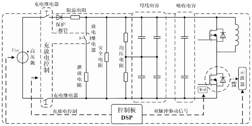
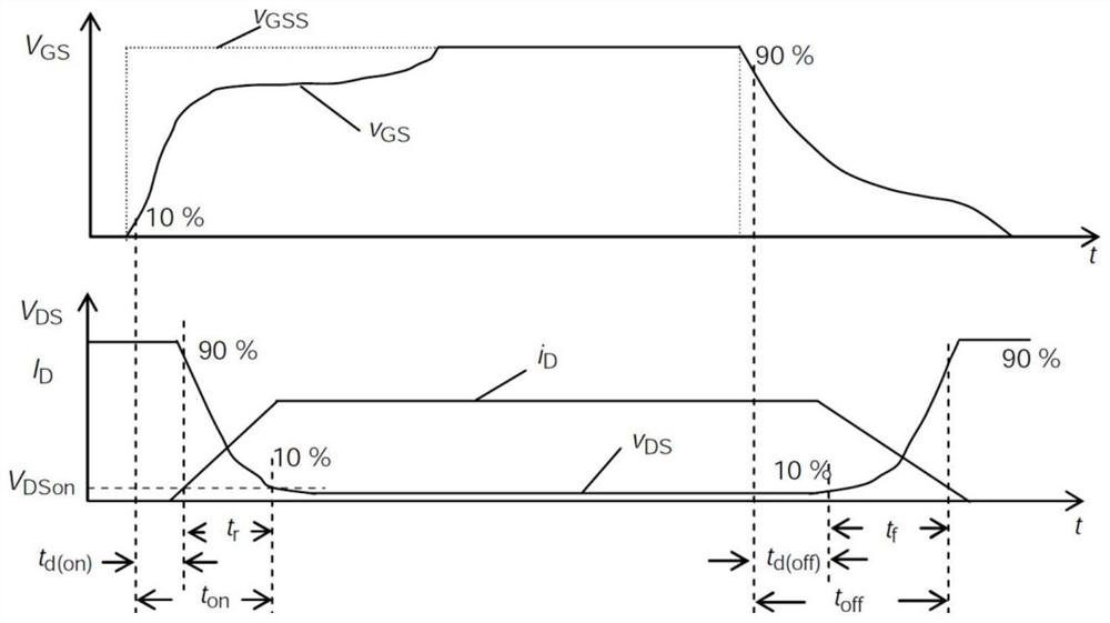
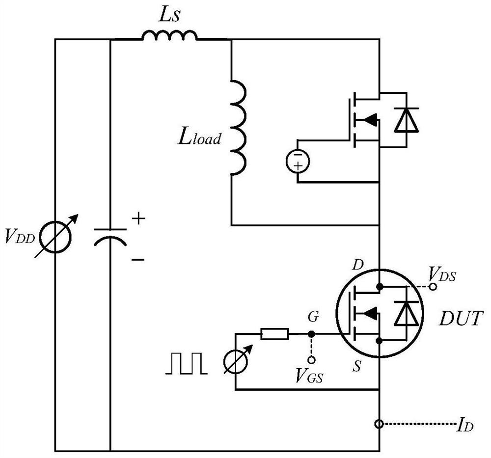
[0071] Such as Figure 1-Figure 3 As shown, a power semiconductor characteristic parameter test syste...


PUM


Abstract

The invention discloses a power semiconductor characteristic parameter testing system and method, and belongs to the technical field of semiconductor characteristic parameter testing. The invention discloses a power semiconductor characteristic parameter testing system which comprises a power main loop, a double-pulse testing circuit and an inductance blocking circuit. According to the invention, an auxiliary power semiconductor is arranged to control the conduction time of the to-be-tested power semiconductor and the on-off of the circuit, and absorption capacitors are arranged at the two ends of the power semiconductor, so that partial parasitic inductance between the bus capacitor and the test half-bridge can be effectively blocked; and meanwhile, a power main loop is arranged by adopting a laminated busbar structure, stray inductance is greatly reduced through a smaller loop area, and high current bearing can be realized with lower voltage. Therefore, voltage overshoot superposition and switching loss can be effectively reduced, electromagnetic interference can be effectively avoided, and the system and methodare especially suitable for high-precision dynamic characteristic parameter testing of a third-generation semiconductor high-voltage SiC power device.

Description

technical field [0001] The invention relates to a power semiconductor characteristic parameter testing system and method, belonging to the technical field of semiconductor characteristic parameter testing. Background technique [0002] The use of a high proportion of power electronic equipment is the main technical feature of the new generation of power systems. With a large number of different types and different voltage levels of power electronic equipment connected to the grid, the trend of power electronics in my country's power system is gradually emerging. Power electronics is an important supporting technology for modern science, industry and national defense, and one of the core technologies for transforming traditional industries and developing emerging industries. Power devices are the core and foundation of power electronics technology, the core driving force for the development of power electronics technology, and largely determine the performance of power elect...

Claims


Application Information

Patent Timeline
Patent Type & Authority Applications(China)
IPC IPC(8): G01R31/26
CPCG01R31/2607G01R31/2601
Inventor 王异凡龚金龙宋琦华孙明王一帆骆丽王尊刘黎邵先军王少华陈虔曾明全李文燕邓志江张斌林氦郭清陈少华
Owner ELECTRIC POWER RES INST OF STATE GRID ZHEJIANG ELECTRIC POWER COMAPNY
Features
  • R&D
  • Intellectual Property
  • Life Sciences
  • Materials
  • Tech Scout
  • Unparalleled Data Quality
  • Higher Quality Content
  • 60% Fewer Hallucinations
Learn More