Nanowire-plasmon coupled single photon emitter and preparation method thereof

A technology of plasmons and nanowires, which is applied in the field of quantum communication, can solve the problems of excessive minimum radius of nanowires, large system structure size, and difficulty in integration, etc., so as to improve single-photon emission rate, increase spontaneous emission rate, and stabilize Emission rate effect

Active Publication Date: 2022-01-04
UNIV OF ELECTRONICS SCI & TECH OF CHINA
View PDF9 Cites 0 Cited by
  • Summary
  • Abstract
  • Description
  • Claims
  • Application Information

AI Technical Summary

Problems solved by technology

However, this method has two main disadvantages: First, the enhancement effect of nanowires on the spontaneous emission rate of quantum dots is limited, and even when the nanowire radius is low, it cannot support the lowest mode transmission of cylindrical waveguides, thus greatly suppressing Spontaneous emission of quantum dots (0.02 times the original)
Second, the required minimum radius of the nanowire is too large, resulting in a large size of the final system structure, which is difficult to integrate

Method used


Image

  • Nanowire-plasmon coupled single photon emitter and preparation method thereof
  • Nanowire-plasmon coupled single photon emitter and preparation method thereof
  • Nanowire-plasmon coupled single photon emitter and preparation method thereof

Examples


preparation example Construction

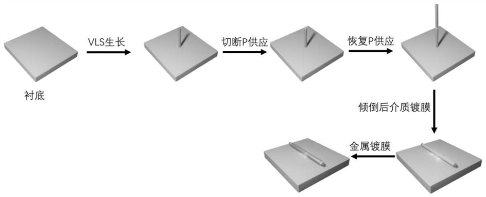
[0036] The present invention also provides a method for preparing the above nanowire-plasmon coupled single photon emitter, comprising the following steps:

[0037] S1 provides a substrate;

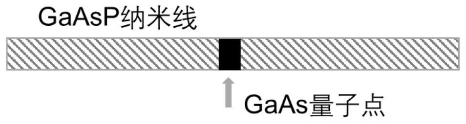
[0038] S2 grow the nanowire body on the substrate; when growing to the height of the quantum dot, replace it with the component growth of the quantum dot, continue to grow the nanowire body until the growth of the nanowire body is completed after the growth of the quantum dot is completed;

[0039] S3 uses an ultrasonic sounder to pour the nanowire body into a horizontal direction;

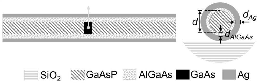
[0040] S4 uses electron beam evaporation to perform dielectric coating on the nanowire body;

[0041] S5 uses electron beam evaporation to coat the nanowire body with a metal film.

[0042] Preferably, the VLS process is used to grow the nanowire body in the S2 step. VLS is the vapor-liquid-solid process. The impurities in the system can form eutectic catalyst droplets with other components, and the gas raw...

Embodiment 1

[0051] A kind of high-efficiency single-photon emitter described in the present embodiment, its preparation method is as follows:

[0052] (1) provide a substrate, the material of the substrate is silicon dioxide;

[0053](2) The GaAsP nanowire body is grown on the silicon wafer of the substrate by a Ga-assisted VLS process, the growth temperature is 630° C., and the growth time is 60 minutes. GaAs quantum dot regions are formed in the middle of GaAsP by cutting off the P supply during growth. And increase the beam pressure to compensate for the decrease of phosphorus supply during QD growth. The growth time of QD is 30s. After QD growth, the equivalent beam pressure of As and P molecules returns to the initial state, and the preparation of the nanowire body and quantum dots is completed.

[0054] (3) using an ultrasonic sounder to pour the prepared sample;

[0055] (4) Electron beam evaporation is used to carry out dielectric coating on the sample, the thickness is 10nm, ...

Embodiment 2

[0059] A kind of high-efficiency single-photon emitter described in the present embodiment, its preparation method is as follows:

[0060] (1) provide a substrate, the material of the substrate is silicon dioxide;

[0061] (2) The GaAsP nanowire body is grown on the silicon wafer of the substrate by a Ga-assisted VLS process, the growth temperature is 630° C., and the growth time is 60 minutes. GaAs quantum dot regions are formed in the middle of GaAsP by cutting off the P supply during growth. And increase the beam pressure to compensate for the decrease of phosphorus supply during QD growth. The growth time of QD is 30s. After QD growth, the equivalent beam pressure of As and P molecules returns to the initial state, and the preparation of the nanowire body and quantum dots is completed.

[0062] (3) using an ultrasonic sounder to pour the prepared sample;

[0063] (4) Electron beam evaporation is used to carry out dielectric coating on the sample, the thickness is 10nm,...


PUM

PropertyMeasurementUnit
thicknessaaaaaaaaaa
thicknessaaaaaaaaaa
thicknessaaaaaaaaaa

Abstract

The invention discloses a nanowire-plasmon coupled single photon emitter. The nanowire-plasmon coupled single photon emitter comprises a substrate, a nanowire body arranged on the substrate, a dielectric coating film annularly wrapping the nanowire body, and a metal coating film annularly wrapping the dielectric coating film, and a quantum dot is disposed on the nanowire body. According to the nanowire-plasmon coupled single-photon emitter structure provided by the invention, nanowires are prepared in a substrate, quantum dots are prepared in the middle in a doping manner, and medium coating and metal coating are performed on the prepared nanowire quantum dots. The metal plasmons are coupled with the quantum dots, so that the single-photon emission rate of the emitter is improved, and the minimum radius of single-mode transmission supported by the nanowires is effectively reduced. Due to the adoption of a coating method, the structure can be self-assembled, so that the position of the quantum dots is controllable. According to the invention, a stable single photon source with a high emission rate can be obtained.

Description

technical field [0001] The invention relates to the field of quantum communication, in particular to a nanowire-plasmon coupled single-photon emitter and a preparation method thereof. Background technique [0002] Single photon emitters are one of the key building blocks in quantum communication, quantum computing and quantum metrology. Quantum dots (QD, Quantum dots), as a typical two-level system, have become the most promising single-photon emitters due to their broadband absorption, narrow emission bands, spectral tunability, and stable and bright photoluminescence properties. one. However, the application of single quantum dots is limited due to their low spontaneous emission rate (approximately 10ns, 100MHz) and random emission directions. To increase the spontaneous emission (SE) rate of excited states and thus the maximum single-photon rate, the emitter can be placed in the photon environment to increase its local density of optical states. This increased rate of ...

Claims


Application Information

Patent Timeline
Patent Type & Authority Applications(China)
IPC IPC(8): H01S5/34H01S5/343G02B5/00H04B10/50H04B10/70B82Y30/00B82Y40/00
CPCH01S5/3412H01S5/343G02B5/008H04B10/70H04B10/501B82Y30/00B82Y40/00Y02P70/50
Inventor 李佩航余鹏王志明
Owner UNIV OF ELECTRONICS SCI & TECH OF CHINA
Why Eureka
Try Eureka