Low-leakage amplifier biasing circuit

A bias circuit and amplifier technology, applied in amplifiers, parts of amplifying devices, improving amplifiers to reduce temperature/power supply voltage changes, etc. The effect of reducing static power consumption

Active Publication Date: 2022-01-04
南京燧锐科技有限公司
View PDF12 Cites 0 Cited by
  • Summary
  • Abstract
  • Description
  • Claims
  • Application Information

AI Technical Summary

Problems solved by technology

[0006] figure 2 It is the common source bias circuit diagram of the existing MOSFET transistor RF amplifier, such as figure 2 As shown, when the gate terminal of the MOSFET is pulled down to the ground, if there is still a voltage Vd at the drain terminal, the transistor still has the reverse saturatio

Method used


Image

  • Low-leakage amplifier biasing circuit
  • Low-leakage amplifier biasing circuit
  • Low-leakage amplifier biasing circuit

Examples


Example Embodiment

[0040] Example 1

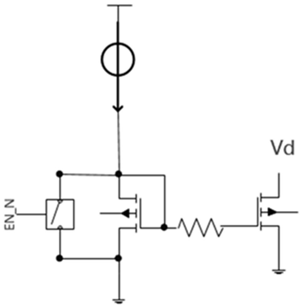
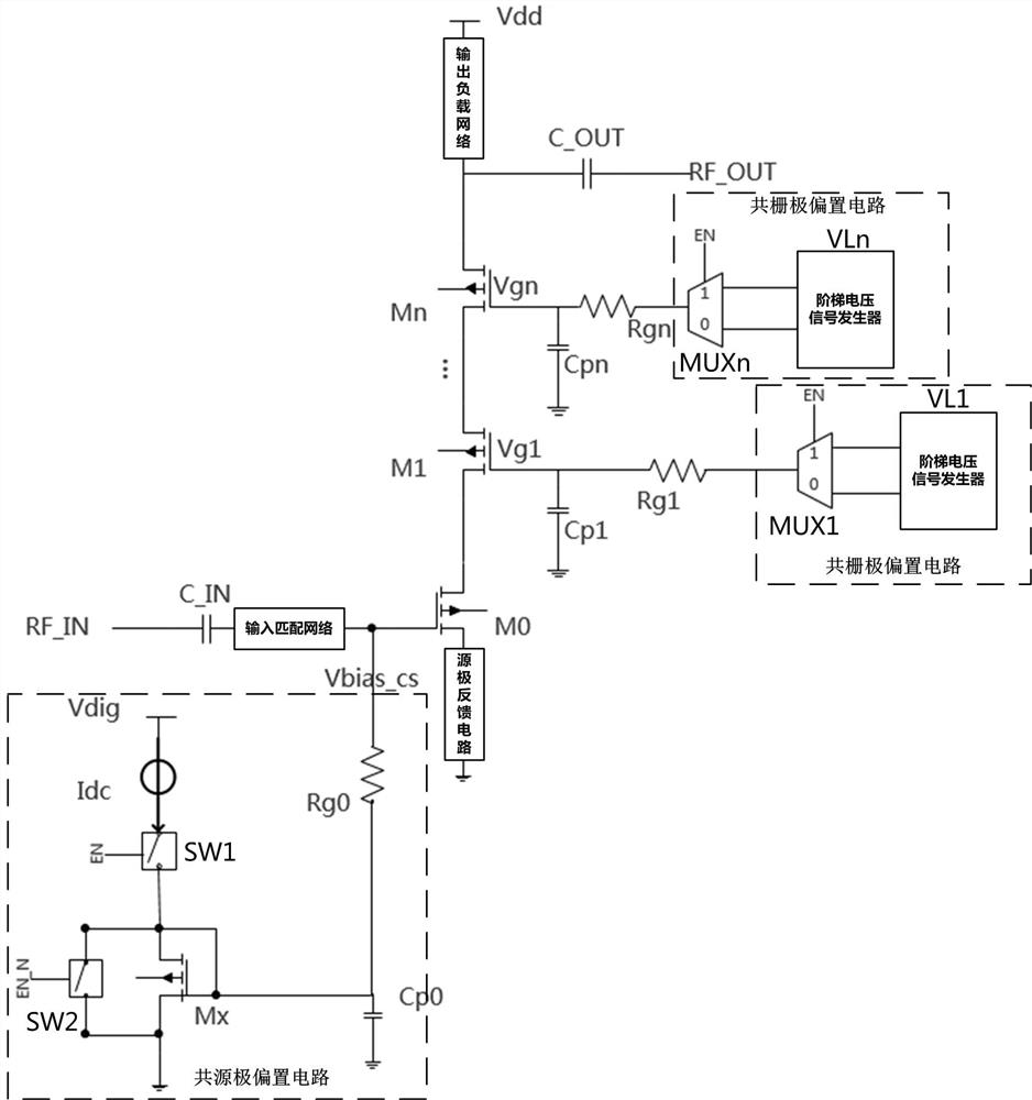
[0041] Figure 4 It is the bias circuit diagram of the low leakage amplifier according to the present invention, such as Figure 4 As shown, the low leakage amplifier bias circuit of the present invention includes a common source bias circuit and a plurality of common gate bias circuits, wherein,

[0042] The common source bias circuit, the output end of which is connected to the gate of the common source transistor M0 of the amplifier, provides source bias voltage for the common source transistor M0 of the amplifier.

[0043] A plurality of common-gate bias circuits are respectively connected to the gates of the common-gate transistors M1~Mn of the amplifier through the isolation resistors Rg1-Rgn to provide the common-gate bias voltage Vg1~Mn for the multiple common-gate transistors M1~Mn of the amplifier. Vgn.

[0044] In the embodiment of the present invention, the common source bias circuit includes a common source bias transistor Mx, a current sourc...

Example Embodiment

[0053] Example 2

[0054] Figure 5 It is a circuit diagram of a ladder voltage signal generator according to the present invention, such as Figure 5 As shown, the ladder voltage signal generator (VL1-VLn) of the present invention includes a plurality of resistors (R0-Rn) with the same resistance value connected in series to divide the voltage of the logic power supply (Vdig), and extract the intermediate node to turn on the gate voltage Vgn and The turn-off voltage Voff is used as the common gate bias voltage:

[0055] Vgn=(n-1) / n*Vdig,

[0056] Voff=1 / n*Vdig,

[0057] In actual situations, any node Vg can be selected, wherein Vgn is the turn-on gate voltage, and Voff is the turn-off voltage.

Example Embodiment

[0058] Example 3

[0059] Image 6 It is the gate circuit diagram according to the present invention, such as Image 6 As shown, the gating device (MUX1-MUXn) of the present invention is realized by two sets of NMOS and PMOS switches:

[0060] Vout=Vgn*EN+Voff*(1-EN),

[0061] When EN=1, the amplifier is enabled, and the strobe (MUX1-MUXn) outputs the on-gate voltage Vgn to the gate; when EN=0, the amplifier is turned off, and the strobe (MUX1-MUXn) outputs the off-voltage Voff.

[0062] In the embodiment of the present invention, the common-source bias circuit forms a current mirror by the common-source bias transistor Mx and the common-source transistor M0 of the amplifier, and the amplification part of the amplifier is the same as that of the existing amplifier.

[0063] In amplifier off state, EN=0:

[0064] The first switch SW1 is turned off, the current source Idc is turned off, the second switch SW2 is turned on, and the common source bias voltage Vbias_cs is pulled...


PUM


Abstract

A low-leakage amplifier bias circuit comprises a common-source bias circuit and a plurality of common-gate bias circuits; the common-source bias circuit provides common-source bias voltage for a common-source transistor of an amplifier, and the common-gate bias circuits provide common-source bias voltage for a common-source transistor of the amplifier; the common-gate bias circuit provides bias voltage for a common-gate transistor of the amplifier; when the amplifier is in a turn-off state, the common source bias circuit pulls down the common source bias voltage to the ground, and the common gate bias circuit pulls down the bias voltage to turn-off voltage; when the amplifier is in a turn-off and turn-on state, the common-source bias circuit disconnects the common-source bias voltage from the ground, and the common-gate bias circuit pulls the bias voltage to turn-on gate voltage. According to the low-leakage amplifier biasing circuit, the grid voltage of the common-gate transistor of the amplifier is lowered, so that the drain voltage of the common-source transistor is lowered, the leakage current is controlled to the maximum extent, and the static power consumption of the amplifier is lowered.

Description

technical field [0001] The present invention relates to an amplifier, in particular to an amplifier bias circuit. Background technique [0002] Metal-Oxide-Semiconductor Field-Effect Transistor (MOSFET) is a field-effect transistor (field-effect transistor) that can be widely used in analog circuits and digital circuits, including CMOS, SOI, GaN , BJT, etc. [0003] For MOSFET transistors, when both the drain and source are grounded, as the gate voltage VG increases, electrons are attracted by the positive electricity on the gate, forming a depletion layer between the drain and source. At this time The MOSFET is in the off state; as the gate voltage increases, more electrons are attracted to the surface of the gate oxide layer, forming a conduction channel between the drain and the source. current. But when the drain voltage is not 0, even if VG=0, it does not mean that there is no current generation in the MOSFET. Since the PN junction is formed between the drain N regi...

Claims


Application Information

Patent Timeline
IPC IPC(8): H03F1/02H03F1/30H03F3/16
CPCH03F1/0205H03F1/301H03F3/16H03F2200/522H03F2200/525
Inventor 马昊泽李南陆建华
Owner 南京燧锐科技有限公司
Why Eureka
Try Eureka