

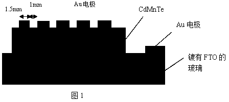
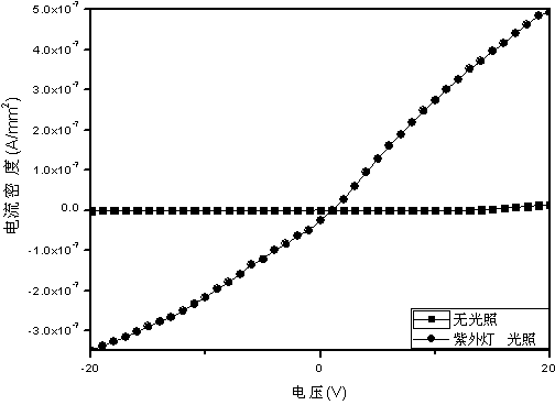
Method for manufacturing CdMnTe film ultraviolet-light detector of ohm structure
A detector and ultraviolet light technology, applied in the direction of semiconductor devices, final product manufacturing, sustainable manufacturing/processing, etc., to achieve the effects of reducing noise, controlling device leakage current, and improving device leakage current
- Summary
- Abstract
- Description
- Claims
- Application Information
AI Technical Summary
Problems solved by technology
Method used
Image


Examples
Embodiment 1
[0024] The preparation process and steps of this embodiment are as follows:
[0025] (a) Preparation of CdMnTe single crystal sublimation source: According to the known prior art, the molar content of high-purity Cd, Mn and Te is 50% for Te, 44% for Cd, and 6% for Mn Put the compound into a quartz tube, and grow a CdMnTe single crystal with good quality and relatively uniform composition distribution under high vacuum by using the mobile heating method, and use the grown crystal slice as the sublimation source;
[0026] (b) Substrate pretreatment: use glass coated with a transparent conductive layer FTO as the substrate, and ultrasonically clean the substrate with deionized water, acetone and ethanol for 15 minutes respectively to remove impurities and organic substances on the surface, dry and put Into the close space sublimation reaction chamber;
[0027] (c) CdMnTe film growth process: turn on the mechanical pump to evacuate, pump the air pressure in the sublimation ch...
Embodiment 2
[0031] The preparation process and steps of this embodiment are as follows:
[0032] (a) Preparation of CdMnTe single crystal sublimation source: According to the known prior art, high-purity Cd, Mn, and Te are prepared with the molar content of Te being 50%, the molar content of Cd being 44%, and the Mn content being 6% Put the compound into a quartz tube, and grow a CdMnTe single crystal with good quality and relatively uniform composition distribution under high vacuum by using the mobile heating method, and use the grown crystal slice as the sublimation source;
[0033] (b) Substrate pretreatment: use glass coated with a transparent conductive layer FTO (fluorine tin oxide) as the substrate, and ultrasonically clean the substrate with deionized water, acetone and ethanol for 15 minutes respectively to remove impurities and organic matter on the surface , put into near-space sublimation reaction chamber after drying.
[0034](c) CdMnTe thin film growth process: Turn on...
Embodiment 3
[0038] The preparation process and steps of this embodiment are as follows:
[0039] (a) Preparation of CdMnTe single crystal sublimation source: According to the known prior art, the molar content of high-purity Cd, Mn and Te is 50% for Te, 44% for Cd, and 6% for Mn. % complexes were placed in a quartz tube, and under high vacuum, a CdMnTe single crystal with good quality and relatively uniform composition distribution was grown by moving heating method, and the grown crystal slice was used as a sublimation source;
[0040] (b) Substrate pretreatment: use glass coated with a transparent conductive layer FTO as the substrate, and ultrasonically clean the substrate with deionized water, acetone and ethanol for 15 minutes respectively to remove impurities and organic substances on the surface, dry and put Into the close space sublimation reaction chamber;
[0041] (c) CdMnTe film growth process: turn on the mechanical pump to evacuate, pump the air pressure in the sublimati...
PUM
 Abstract
Description
Claims
Application Information