
Inverted light emitting diode

A light-emitting diode and flip-chip technology, which is applied in the direction of electrical components, circuits, semiconductor devices, etc., can solve the problems of abnormal golden explosion point, poor compactness, failure of flip-chip light-emitting diodes, etc., achieve small thickness, improve reliability, Improve coverage continuity

Active Publication Date: 2022-01-07
QUANZHOU SANAN SEMICON TECH CO LTD
View PDF6 Cites 2 Cited by
  • Summary
  • Abstract
  • Description
  • Claims
  • Application Information

AI Technical Summary

Problems solved by technology

When the metal electrode is covered with an insulating layer, since the overall thickness of the metal electrode is relatively thick, the insulating layer above the side wall of the metal electrode has poor compactness. Migration of less dense regions in the layer, leading to failure of flip-chip LEDs
Moreover, the gold layer often contains undissolved gold particles, which are prone to abnormal gold burst points.
[0005] Based on the technical problems involved in the above-mentioned metal electrodes, the performance of traditional flip-chip light-emitting diodes can no longer meet the high reliability requirements of backlight applications or display applications, as well as small-sized flip-chip light-emitting diodes.

Method used


Image

  • Inverted light emitting diode
  • Inverted light emitting diode
  • Inverted light emitting diode

Examples


Embodiment Construction

[0042] The implementation of the present application is described below through specific specific examples, and those skilled in the art can easily understand other advantages and effects of the present application from the content disclosed in this specification. The present application can also be implemented or operated through other different specific implementation modes, and various modifications or changes can be made to the details in the present application based on different viewpoints and applications without departing from the spirit of the present application.

[0043] In the description of this application, it should be noted that the orientation or positional relationship indicated by the terms "upper" and "lower" are based on the orientation or positional relationship shown in the attached drawings, or the usual placement of the application product when it is used. Orientation or positional relationship is only for the convenience of describing the present appli...


PUM

PropertyMeasurementUnit
thicknessaaaaaaaaaa
thicknessaaaaaaaaaa
thicknessaaaaaaaaaa

Abstract

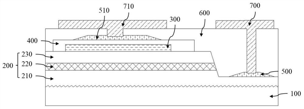
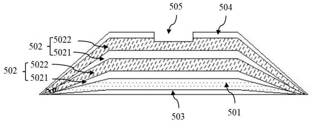
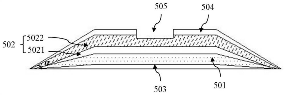
The invention discloses an inverted light-emitting diode which comprises a semiconductor stacking layer, a first metal electrode and a second metal electrode, the first metal electrode and the second metal electrode are located on the semiconductor stacking layer, and each of the the first metal electrode and the second metal electrode is of a gold-free laminated structure. The gold-free laminated structure comprises an aluminum reflecting layer and at least one platinum metal layer located on the upper surface of the aluminum reflecting layer. According to the invention, the first metal electrode and the second metal electrode are arranged to be of a gold-free laminated structure, so that the abnormal phenomenon caused by gold layers in the first metal electrode and the second metal electrode can be avoided, the thickness is small, the coverage continuity of an insulating layer above the surface of the electrode and the coverage continuity of a bonding pad can be improved, and the reliability of the inverted light-emitting diode is improved.

Description

technical field [0001] The present application relates to the technical field related to light-emitting diodes, and in particular to a flip-chip light-emitting diode. Background technique [0002] Due to the characteristics of high luminous efficiency, energy saving, environmental protection, and long life, flip-chip light-emitting diodes are widely used in various fields, such as lighting and backlighting. Among them, compared with other display technologies currently popular in the industry, the small-size flip-chip LED backlight technology has the biggest advantage in that it has no scientific problems in materials, and it is the easiest and fastest to be mass-produced and put into the market. [0003] A traditional flip-chip light-emitting diode includes a semiconductor layer, a metal electrode and a pad, wherein the metal electrode is located inside and contacts the surface of the semiconductor layer or the surface of the transparent conductive layer on the semiconducto...

Claims


Application Information

Patent Timeline
Patent Type & Authority Applications(China)
IPC IPC(8): H01L33/38H01L33/40
CPCH01L33/38H01L33/405H01L33/486H01L33/40H01L33/12H01L33/382H01L33/62
Inventor 黄敏詹宇夏章艮洪灵愿林素慧张中英
Owner QUANZHOU SANAN SEMICON TECH CO LTD
Learn More