Flip red light diode chip and preparation method thereof

A diode and red light technology, which is applied in the direction of electrical components, circuits, semiconductor devices, etc., can solve the problems that affect the light output efficiency of red light emitting diodes, lattice mismatch, and the quality of red light emitting diode chips is not ideal, so as to improve the light output Efficiency, reduced thermal stress, good adhesion effect

Active Publication Date: 2022-01-07
HC SEMITEK ZHEJIANG CO LTD
View PDF8 Cites 1 Cited by
  • Summary
  • Abstract
  • Description
  • Claims
  • Application Information

AI Technical Summary

Problems solved by technology

[0003] The epitaxial layer grown on the substrate in the epitaxial wafer is limited to the lattice mismatch between the substrate and the epitaxial material and the internal stress, resulting in the quality of the obtained red light emitting diode chip is still not ideal, affecting the final red light emitting diode chip. Light Efficiency of Light Emitting Diodes

Method used


Image

  • Flip red light diode chip and preparation method thereof
  • Flip red light diode chip and preparation method thereof
  • Flip red light diode chip and preparation method thereof

Examples


Embodiment Construction

[0036] In order to make the purpose, technical solution and advantages of the present disclosure clearer, the implementation manners of the present disclosure will be further described in detail below in conjunction with the accompanying drawings.

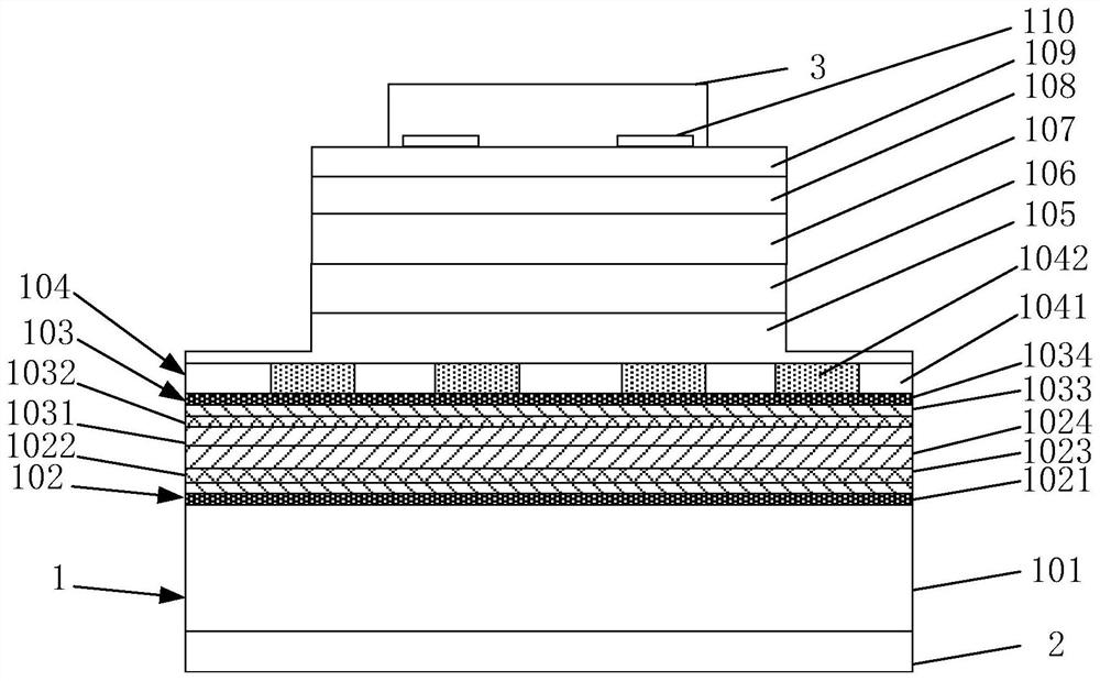
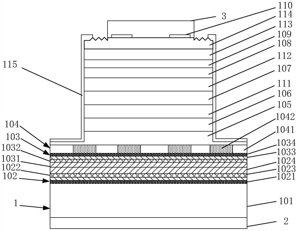
[0037] figure 1 It is a schematic structural diagram of a flip-chip red light-emitting diode chip provided by an embodiment of the present disclosure. Refer to figure 1 It can be seen that the embodiment of the present disclosure provides a flip-chip red light diode chip, and the flip-chip red light diode chip includes an epitaxial wafer 1 , a p-electrode 2 and an n-electrode 3 .

[0038] The epitaxial wafer 1 includes a support substrate 101 and a substrate bonding metal layer 102, an epitaxial bonding metal layer 103, a reflective layer 104, a p-GaP ohmic contact layer 105, and a p-AlInP confinement layer stacked sequentially on the support substrate 101. 106 , an active layer 107 , an n-AlInP confinement layer 108 , an n-AlGaIn...


PUM

PropertyMeasurementUnit
thicknessaaaaaaaaaa
thicknessaaaaaaaaaa
thicknessaaaaaaaaaa

Abstract

The invention provides a flip red light diode chip and a preparation method thereof, and belongs to the technical field of light emitting diodes. After a substrate bonding metal layer and an epitaxial bonding metal layer are bonded on a supporting substrate, the supporting substrate supports an epitaxial structure on the epitaxial bonding metal layer, and the substrate bonding metal layer comprises a substrate Cr metal sub-layer, a substrate Pt metal sub-layer, a substrate Ag metal sub-layer and a substrate In metal sub-layer which are stacked in sequence; the epitaxial bonding metal layer comprises an epitaxial In metal sub-layer, an epitaxial Ag metal sub-layer, an epitaxial Pt metal sub-layer, an epitaxial Ti metal sub-layer and an epitaxial Cr metal sub-layer which are stacked in sequence, and an Ag material effectively reflects light to a light emitting surface. The In metal sub-layer reduces the thermal stress generated by high temperature in an obtained red light diode, so that the quality of the red light diode is improved, and the light emitting efficiency of the red light diode is improved.

Description

technical field [0001] The present disclosure relates to the technical field of light-emitting diodes, in particular to a flip-chip red light-emitting diode chip and a preparation method thereof. Background technique [0002] Red light emitting diode is a common light source device, which is widely used in remote control, vehicle sensing, closed circuit television, etc., and red light emitting diode chip is the basic structure for preparing red light emitting diode. Red light emitting diode chips usually include epitaxial wafers and p, n electrodes. The epitaxial wafer includes a support substrate and n-AlGaInP current spreading layer, n-AlGaInP ohmic contact layer, n-AlInP confinement layer, active layer, p-AlInP confinement layer, Bragg reflector, p -GaP ohmic contact layer. The p-GaP ohmic contact layer has a groove extending to the n-AlGaInP ohmic contact layer, the p-electrode of the red light-emitting diode chip can be arranged on the p-GaP ohmic contact layer, and t...

Claims


Application Information

Patent Timeline
Patent Type & Authority Applications(China)
IPC IPC(8): H01L33/40H01L33/38H01L33/00
CPCH01L33/40H01L33/405H01L33/387H01L33/0062Y02P70/50
Inventor 肖和平朱迪张强
Owner HC SEMITEK ZHEJIANG CO LTD
Why Eureka
Try Eureka