Unlock instant, AI-driven research and patent intelligence for your innovation.

Semiconductor power module packaging structure

A power module and packaging structure technology, applied in the direction of semiconductor devices, semiconductor/solid-state device parts, electric solid-state devices, etc., can solve the problems of complex installation, increased workload, large parasitic capacitance and parasitic inductance, etc., to ensure the working environment , save manpower, improve the cooling effect

Inactive Publication Date: 2022-01-11
汉斯半导体(江苏)有限公司
View PDF0 Cites 0 Cited by
  • Summary
  • Abstract
  • Description
  • Claims
  • Application Information

AI Technical Summary

Problems solved by technology

[0003] In order to solve the problem of large parasitic capacitance and inductance caused by wire bonding and complex internal interconnection structures, the current solution is to use solder to directly connect copper wires to the semiconductor surface. However, if the installed semiconductor Most of the time, the installation is more complicated, which will increase the workload. On the other hand, the heat dissipation effect is not particularly ideal, and a device is needed to solve this problem.

Method used


Image

  • Semiconductor power module packaging structure
  • Semiconductor power module packaging structure
  • Semiconductor power module packaging structure

Examples


Embodiment

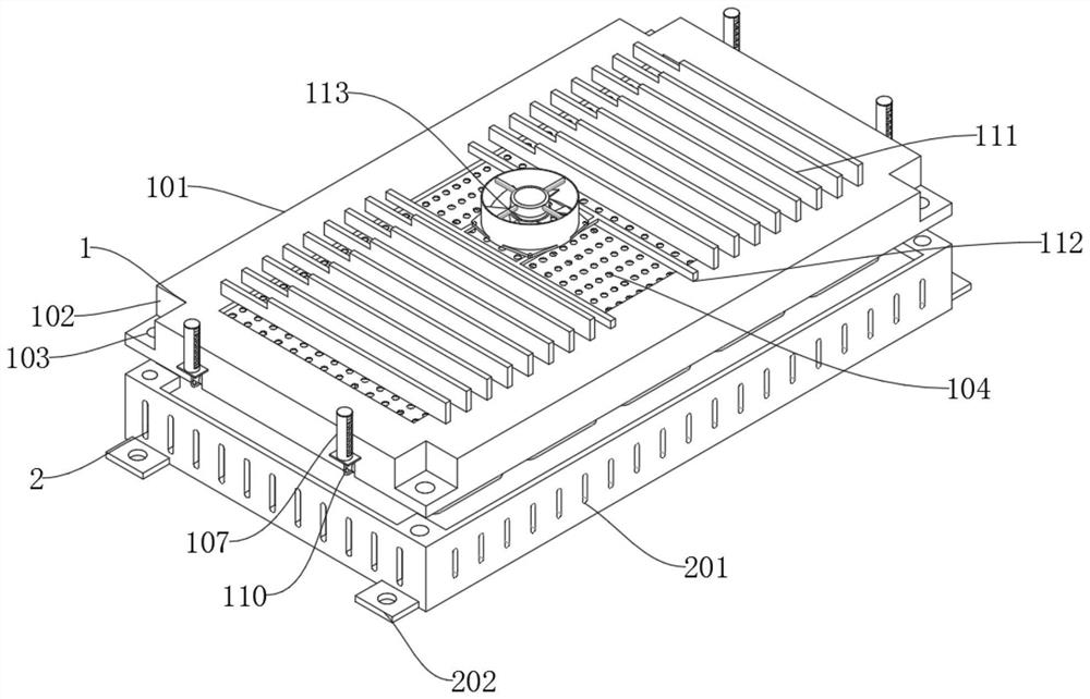
[0031] Such as figure 1 , figure 2 , image 3 , Figure 4 , Figure 5 As shown, the present invention provides a technical solution: a semiconductor power module packaging structure, including a mounting mechanism 1 for packaging and a bearing mechanism 2 for carrying the semiconductor. The mounting mechanism 1 includes a cover plate 101, a mounting groove 102, Upper threaded holes 103, four corners on the cover plate 101 are provided with mounting grooves 102, the mounting grooves 102 are provided with upper threaded holes 103, and the upper end surface of the cover plate 101 is provided with a square mounting hole that penetrates up and down. An isolation net 104 is detachably and fixedly installed, and two side plates 106 are arranged on both sides of the cover plate 101, and the side of the cover plate 101 is located below the side plate 106. 105, a fixed cylinder 107 is arranged on the upper end surface of the side plate 106, a spring 108 is installed on the inner si...


PUM


Abstract

A semiconductor power module packaging structure disclosed by the present invention comprises a mounting mechanism for packaging and a bearing mechanism for bearing a semiconductor, the mounting mechanism comprises a cover plate, mounting grooves and upper threaded holes, the mounting grooves are formed in the four corners of the cover plate, the upper threaded holes are formed in the mounting grooves, a vertically-through square mounting hole is formed in the upper end face of the cover plate, a separation net is detachably and fixedly mounted in the mounting hole, two side plates are arranged on the two side faces of the cover plate, and left-right-through mounting grooves are formed in the positions, below the side plates, of the side faces of the cover plate. The semiconductor power module packaging structure is simple in structure, reasonable in design and low in production cost, connection between the copper wire and the surface of the semiconductor can be facilitated, one-step operation can be achieved, tedious operation is not needed, manpower is greatly saved, meanwhile, the heat dissipation effect of the device is improved, and the working environment of the semiconductor is guaranteed.

Description

technical field [0001] The invention relates to the technical field of semiconductors, in particular to a semiconductor power module packaging structure. Background technique [0002] Semiconductor power modules are widely used in industrial control such as electric transmission and motor control, automobile drive and hybrid power, wind energy, welding machine, locomotive traction and many other fields, to convert the input direct current (DC) into three-phase alternating current (AC) output, as Various switching power supplies. [0003] In order to solve the problem of large parasitic capacitance and inductance caused by wire bonding and complex internal interconnection structures, the current solution is to use solder to directly connect copper wires to the semiconductor surface. However, if the installed semiconductor Most of the time, the installation is relatively complicated, which will increase the workload. On the other hand, the heat dissipation effect is not parti...

Claims


Application Information

Patent Timeline
Patent Type & Authority Applications(China)
IPC IPC(8): H01L23/10H01L23/367H01L23/467H01L23/38H01L23/00
CPCH01L23/10H01L23/367H01L23/467H01L23/38H01L23/564
Inventor 韩波
Owner 汉斯半导体(江苏)有限公司
Features
  • R&D
  • Intellectual Property
  • Life Sciences
  • Materials
  • Tech Scout
  • Unparalleled Data Quality
  • Higher Quality Content
  • 60% Fewer Hallucinations
Learn More