Laser fragmentation method for solid material

A solid material and laser technology, applied in the direction of electric solid devices, laser welding equipment, semiconductor devices, etc., can solve the problems of high production cost, low production efficiency, complex devices, etc., to improve processing efficiency, increase production efficiency, reduce production cost effect

Pending Publication Date: 2022-01-25
HANS LASER TECH IND GRP CO LTD
View PDF0 Cites 7 Cited by
  • Summary
  • Abstract
  • Description
  • Claims
  • Application Information

AI Technical Summary

Problems solved by technology

[0005] The object of the present invention is to provide a laser slicing method for solid materials, which solves the problems of low production efficiency, high production cost, and complicated devices in the existing solutions, and uses laser to form a peeling surface inside the solid material to be separated to ensure that the thin-layer wafer The thickness is consistent, and the thin-layer wafer obtained after peeling is easy to separate from the solid substrate, which reduces production costs and improves production efficiency

Method used


Image

  • Laser fragmentation method for solid material
  • Laser fragmentation method for solid material
  • Laser fragmentation method for solid material

Examples


Embodiment

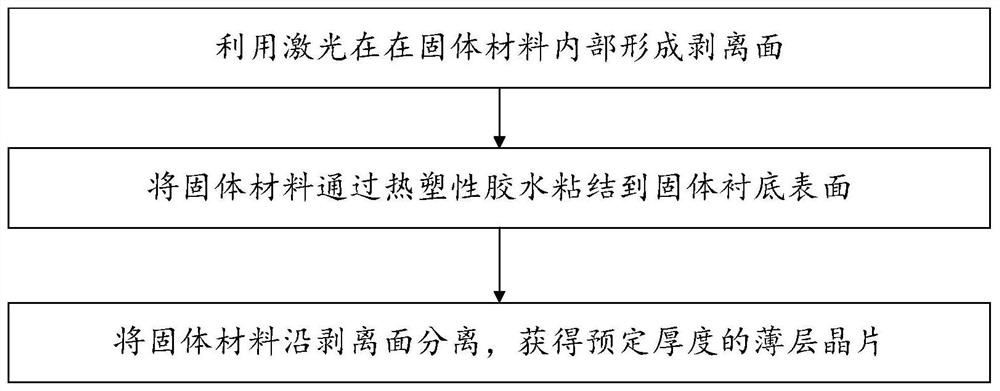
[0046] A laser slicing method for solid materials, such as figure 1 shown, including the following steps:

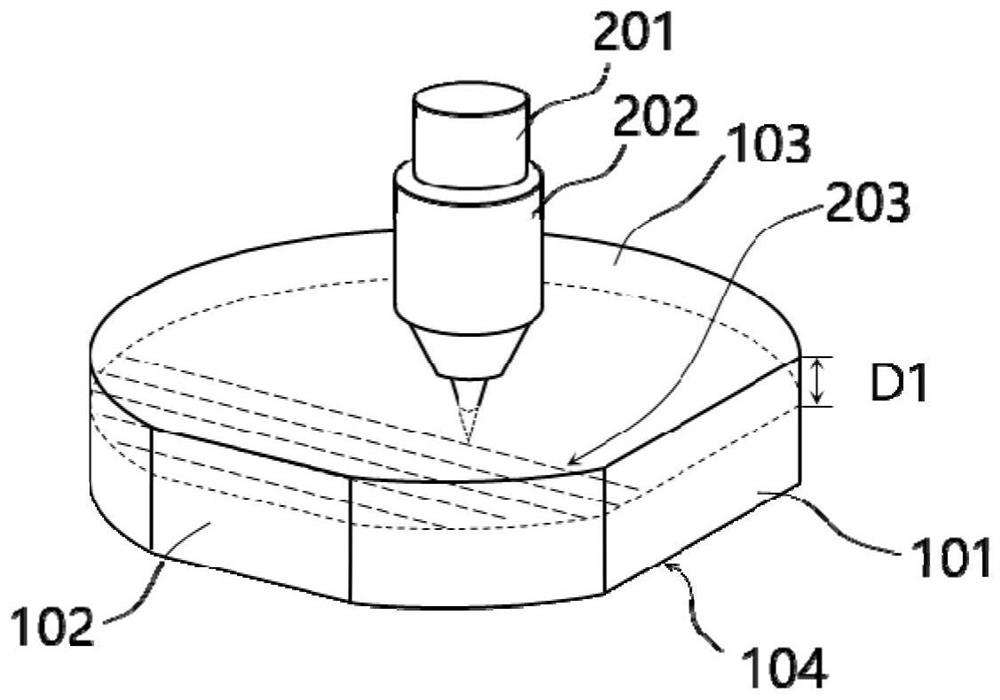
[0047] Use laser to form a peeling surface inside the solid material;

[0048] Bond the solid material to the surface of the solid substrate with thermoplastic glue;

[0049] The solid material is separated along the peeling surface to obtain a thin-layer wafer with a predetermined thickness.

[0050] The laser slicing method for solid materials of the present invention uses laser to form a peeling surface inside the solid material to be separated to ensure the consistency of the thickness of the thin-layer wafer, and uses thermoplastic glue and solid substrate to assist peeling, the peeling process is simple and reliable, and The obtained thin-layer wafer after peeling is easy to separate from the solid substrate, which reduces the production cost and improves the production efficiency.

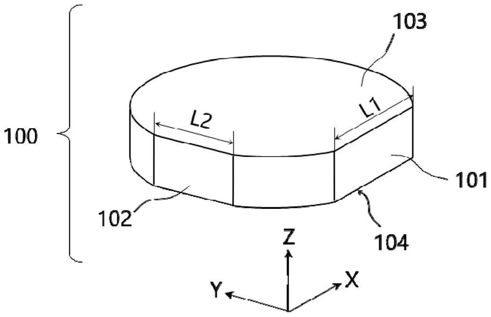
[0051] The solid material is a columnar crystal ingot, the solid material inclu...


PUM

PropertyMeasurementUnit
glass transition temperatureaaaaaaaaaa

Abstract

The embodiment of the invention belongs to the technical field of laser fragmentation, and relates to a laser fragmentation method for a solid material. The technical scheme provided by the invention is that the method comprises the following steps: forming a stripping surface in a solid material by using laser; bonding a solid material to the surface of the solid substrate through thermoplastic glue; and separating the solid material along the stripping surface to obtain a thin-layer wafer with a predetermined thickness. The laser is utilized to form the stripping surface in the solid material to be separated, the consistency of the thickness of the thin-layer wafer is ensured, the thermoplastic glue and the solid substrate are adopted to assist in stripping, the stripping process is simple and reliable, the thin-layer wafer obtained after stripping is easily separated from the solid substrate, the production cost is reduced, and the production efficiency is improved.

Description

technical field [0001] The present application relates to the technical field of laser slicing, and more specifically, to a laser slicing method for solid materials. Background technique [0002] In the preparation of integrated circuit industry and LED industry, silicon carbide (SiC), silicon (Si), sapphire (Al2O3), glass and other materials are usually used as substrates for preparing devices. The traditional wafer preparation method is: using a wire saw to cut the cylindrical ingot into pieces, and then go through the subsequent grinding and thinning process to achieve a specific thickness. However, the above slicing method has serious material loss, and the slicing process will cause most (70-80%) of the crystal ingot to be discarded. Especially for high-hardness SiC materials (Mohs hardness 9.5), the wire sawing method not only consumes a lot of material, but also has many problems such as low efficiency, serious tool wear and environmental pollution, which seriously r...

Claims


Application Information

Patent Timeline
Patent Type & Authority Applications(China)
IPC IPC(8): H01L21/683H01L21/67B23K26/50
CPCH01L21/6835H01L21/67092B23K26/50H01L2221/68386
Inventor 李春昊卢建刚张小军邓正东杨国会陈锐尹建刚高云峰
Owner HANS LASER TECH IND GRP CO LTD
Why Eureka
Try Eureka