

Ldmos device with circular symmetrical structure and its preparation method
A symmetrical structure and circular technology, applied in the field of LDMOS device preparation, can solve the problems of complex manufacturing process and achieve the effect of eliminating process gradient error, reducing edge effect and improving breakdown voltage
- Summary
- Abstract
- Description
- Claims
- Application Information
AI Technical Summary
Problems solved by technology
Method used
Image

Examples
Embodiment Construction
[0043] Specific embodiments of the present invention will be described in detail below in conjunction with the accompanying drawings. It should be understood that the specific embodiments described here are only used to illustrate and explain the present invention, and are not intended to limit the present invention.
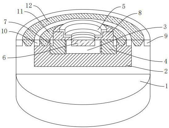
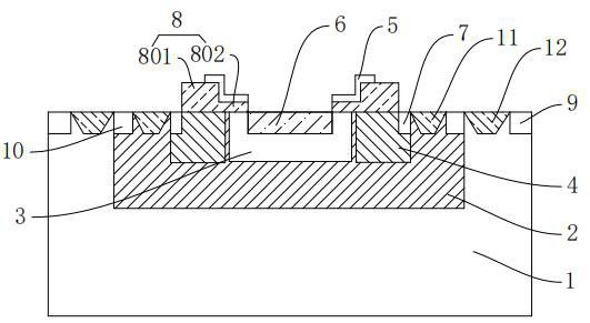
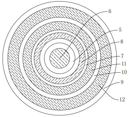
[0044] Such as Figure 1-Figure 3 As shown, the LDMOS device includes: a substrate 1, a gate dielectric layer 8 and a gate electrode 5;
[0045] The substrate 1 is divided into a circular first region, and the first region is formed with a high-voltage well region 2 through ion implantation; the first region includes a circular second region in the center and a circular second region surrounding the second A ring-shaped third region on the periphery of the region; the second region is formed with a body region 3 through ion implantation, and the third region is formed with a drift region 4 through ion implantation, and the drift region 4 and the body region 3 a...
PUM
 Abstract
Description
Claims
Application Information