Controllable metasurface structure based on phase change material and preparation method of controllable metasurface structure
A phase change material and metasurface technology, applied in the field of microelectronics, can solve problems such as limited operating time and complicated control operation, and achieve the effect of small size and thin thickness
- Summary
- Abstract
- Description
- Claims
- Application Information
AI Technical Summary
Problems solved by technology
Method used
Image
Examples
preparation example Construction
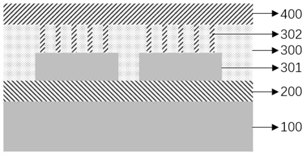
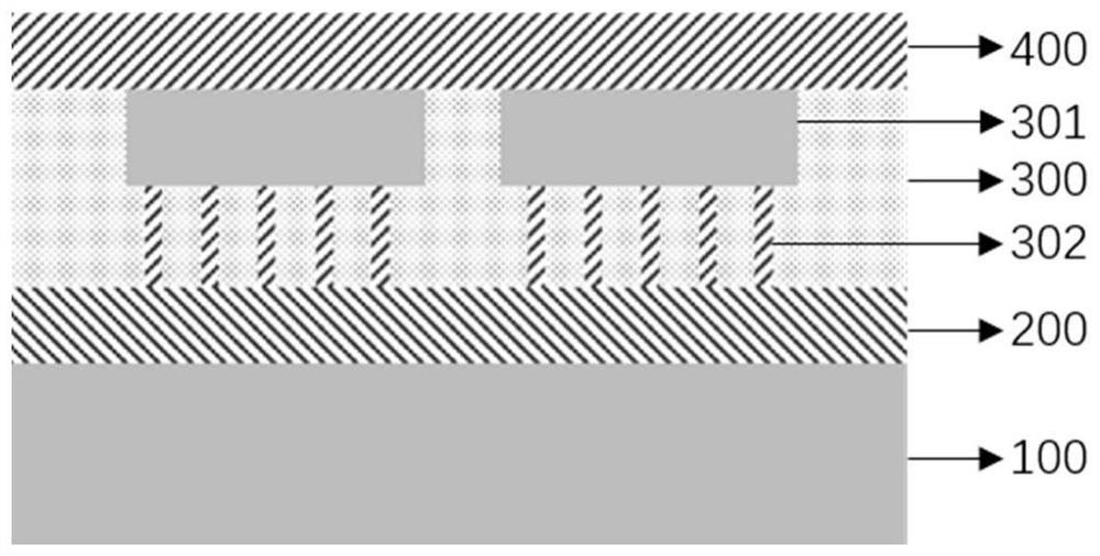
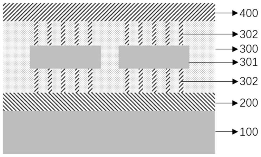
[0048] On the other hand, if Figure 4 As shown, the present invention provides a method for preparing a controllable metasurface structure based on phase change materials, in which microelectrode posts 302 are located between the top electrode layer 400 and the metasurface unit 301, and the preparation method includes the following steps :
[0049] S1-1. Prepare the bottom electrode layer 200 on the substrate 100 . Specifically, the bottom electrode pattern is first designed on the dry and clean substrate 100 by ultraviolet lithography, electron beam lithography or mask method, and then magnetron sputtering, chemical vapor deposition (CVD), chemical vapor phase The bottom electrode material is prepared by transmission (CVT), molecular beam epitaxy (MBE) or electron beam grazing angle deposition (GLAD).
[0050] S1-2. Prepare multiple metasurface units 301 on the bottom electrode layer 200 . Specifically, the metasurface pattern is first designed on the bottom electrode lay...
Embodiment 1
[0071] This embodiment provides a terahertz wave modulator based on a metasurface structure, such as Figure 5 As shown, the device is sequentially arranged from bottom to top: a substrate 100 , a bottom electrode 200 , a transparent insulating layer 300 and a top electrode layer 400 . A plurality of array-arranged metasurface units 301 and a plurality of microelectrode posts 302 are arranged in the transparent insulating layer 300, Figure 5 4 metasurface units are shown in , the upper surface of each metasurface unit 301 is connected to the lower surface of a plurality of microelectrode columns 302, the microelectrode columns 302 on each metasurface unit 301 are arranged in an array, each metasurface unit 301 The lower surface is connected to the bottom electrode 200 , and the upper surface of each microelectrode column 302 is connected to the top electrode layer 400 . Both the metasurface unit 301 and the microelectrode column 302 are cylindrical, the radius of the metasur...
PUM
| Property | Measurement | Unit |
|---|---|---|
| radius | aaaaa | aaaaa |
| thickness | aaaaa | aaaaa |
Abstract
Description
Claims
Application Information


