Light emitting diode and manufacturing method thereof

A technology of light-emitting diodes and silicon dioxide, which is applied in the direction of electrical components, circuits, semiconductor devices, etc., can solve the problems of large difference in refractive index of light-emitting diodes, difficulty in achieving low cost and high efficiency, and limited improvement of light-emitting diodes. Increase the light-emitting area, improve light extraction efficiency, and reduce the effect of total reflection effect

Pending Publication Date: 2022-02-08
XIAMEN SILAN ADVANCED COMPOUND SEMICON CO LTD +1
View PDF6 Cites 0 Cited by
  • Summary
  • Abstract
  • Description
  • Claims
  • Application Information

AI Technical Summary

Problems solved by technology

[0003] The difference in refractive index between the substrate and air in light-emitting diodes is large, resulting in serious total reflection
At present, the backside thinning and coarse grinding process is often used to obtain a substrate surface with a certain roughness, but the above-mentioned methods have a limited effect on improving the light extraction of light-emitting diodes.
In addition, those skilled in the art also use an etching process to pattern the surface of the substrate to reduce the total reflection effect and improve the forward light emission of the light emitting diode. However, due to the high hardness of the substrate and stable chemical properties, it is difficult to achieve low-cost and high-efficiency. Technical solutions

Method used


Image

  • Light emitting diode and manufacturing method thereof
  • Light emitting diode and manufacturing method thereof
  • Light emitting diode and manufacturing method thereof

Examples


Embodiment Construction

[0130] Various embodiments of the invention will be described in more detail below with reference to the accompanying drawings. In the various drawings, the same elements are denoted by the same or similar reference numerals. For the sake of clarity, various parts in the drawings have not been drawn to scale.

[0131] The invention can be embodied in various forms, some examples of which are described below.

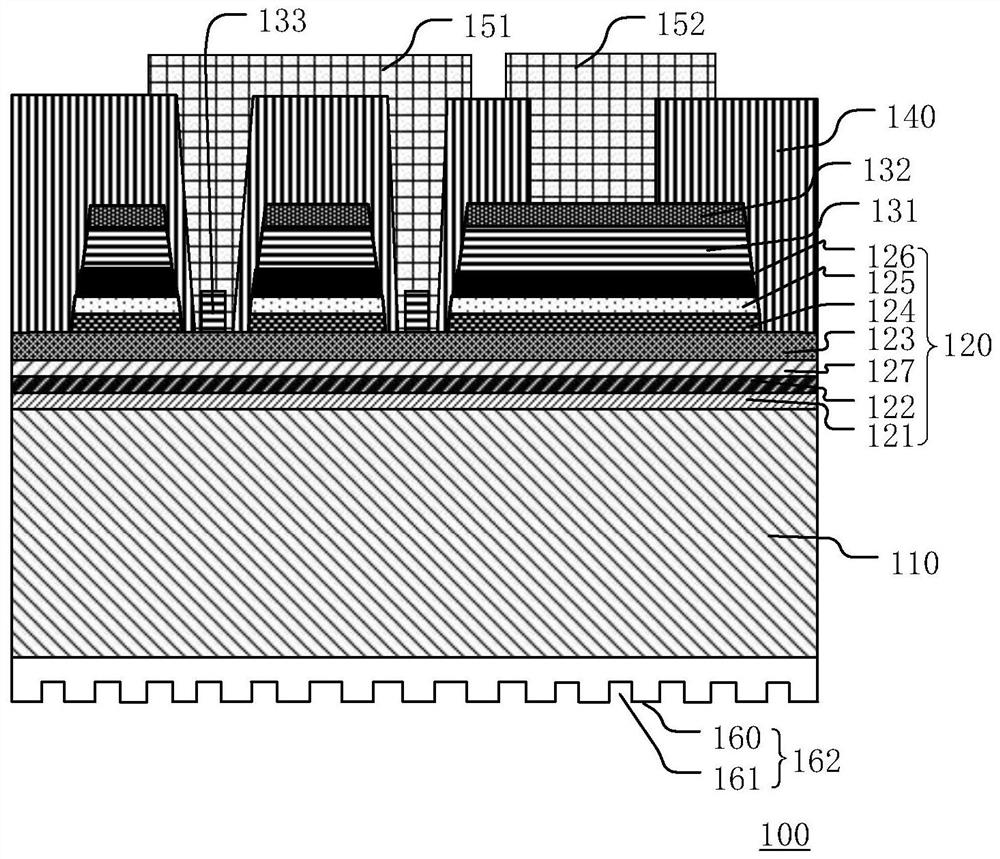
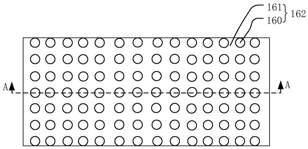
[0132] figure 1 A cross-sectional view of the structure of the light emitting diode provided according to the first embodiment of the present invention is shown. figure 2 A schematic plan view showing the light emitting structure in the light emitting diode according to the first embodiment of the present invention is shown. in, figure 1 for along figure 2 The cross section of line AA.

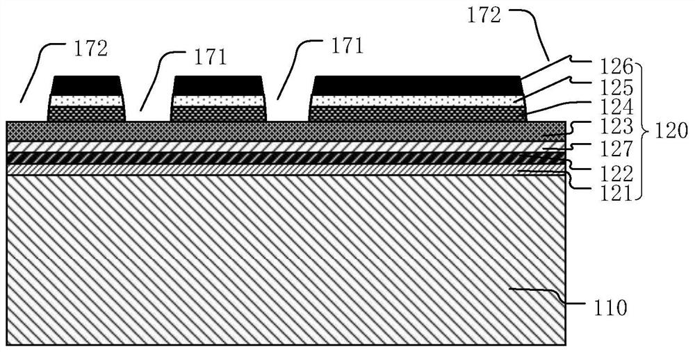
[0133] Such as figure 1 As shown, the light emitting diode 100 is described by taking a deep ultraviolet light emitting diode with a flip-chip through-hole structure as an examp...


PUM

PropertyMeasurementUnit
thicknessaaaaaaaaaa
thicknessaaaaaaaaaa
thicknessaaaaaaaaaa

Abstract

Disclosed are a light emitting diode and a manufacturing method thereof. The light emitting diode comprisres a substrate including a first surface and a second surface opposite to each other; an epitaxial layer located on the first surface of the substrate; and a first dielectric layer located on the second surface of the substrate and at least covering parts of the second surface of the substrate, wherein the refractive index of the first dielectric layer is between the refractive index of the substrate and the refractive index of the air. The first dielectric layer is formed on the second surface of the substrate, and the refractive index of the first dielectric layer is between the refractive index of the substrate and the refractive index of air, so that the refractive index of the light emitting diode from the substrate to the air is gradually reduced through the first dielectric layer, the total reflection effect is reduced, the light extraction efficiency of the light emitting diode is effectively improved, and the optical performance index of the light emitting diode is further improved.

Description

technical field [0001] The invention belongs to the technical field of semiconductor devices, and more specifically relates to a light emitting diode and a manufacturing method thereof. Background technique [0002] A light emitting diode (LED, Light Emitting Diode), as a light emitting element, is often used in a display device, and emits energy by recombining electrons and holes to emit light. Light-emitting diodes can be used as backlights for large-size display screens, smartphones, automotive panels, and notebook computers using white light packaging, or can be combined with red, green, and blue (RGB) LED chips to achieve high CRI. show. [0003] The difference in refractive index between the substrate and air in light-emitting diodes is large, resulting in serious total reflection. At present, the surface of the substrate with a certain roughness can be obtained by using the backside thinning and coarse grinding process, but the above-mentioned means have a limited e...

Claims


Application Information

Patent Timeline
Patent Type & Authority Applications(China)
IPC IPC(8): H01L33/22H01L33/06H01L33/32H01L33/36H01L33/00
CPCH01L33/22H01L33/06H01L33/32H01L33/36H01L33/0075
Inventor 范伟宏毕京锋郭茂峰李士涛马新刚张学双赵进超
Owner XIAMEN SILAN ADVANCED COMPOUND SEMICON CO LTD
Why Eureka
Try Eureka