System-in-package structure, manufacturing method thereof and electronic equipment

A system-level packaging and manufacturing method technology, applied in the field of system-level packaging structure, manufacturing method and electronic equipment, can solve the problems of high cost, low efficiency, complex process, etc., achieve high aspect ratio, low cost, and ease of interface layered effect

Pending Publication Date: 2022-02-18
HUAWEI TECH CO LTD
View PDF0 Cites 1 Cited by
  • Summary
  • Abstract
  • Description
  • Claims
  • Application Information

AI Technical Summary

Problems solved by technology

However, these existing methods still have problems such as complex process, low efficiency or high cost, and need to be further improved

Method used


Image

  • System-in-package structure, manufacturing method thereof and electronic equipment
  • System-in-package structure, manufacturing method thereof and electronic equipment
  • System-in-package structure, manufacturing method thereof and electronic equipment

Examples


Embodiment 1

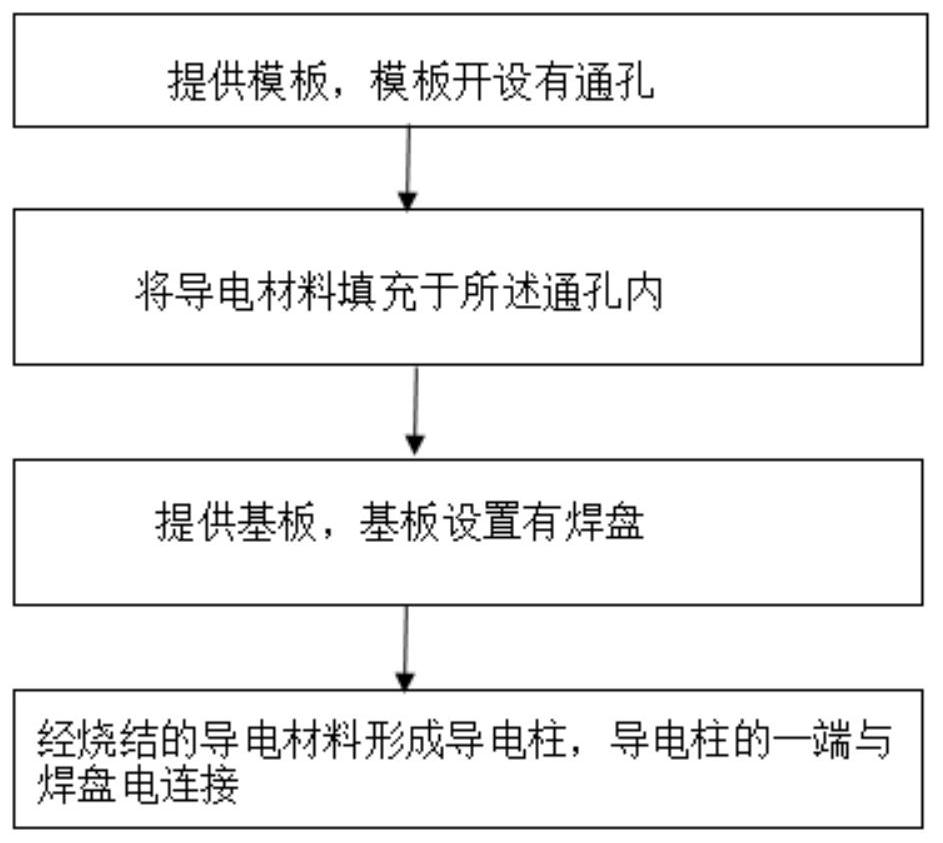
[0155] Figure 9 shows a schematic flow chart of the manufacturing method of the system-in-package structure provided by Embodiment 1, as Figure 9 shown.

[0156] S100. Template making: use silicone resin materials to make a template that can withstand high temperatures of 250°C and can be reused. The template is provided with an array of through holes corresponding to the array of pads on the back of the double-sided SiP substrate. The array of through holes can be up and down. The through-hole arrays are respectively arranged in two rows, and the left and right sides are respectively arranged in a form of a column. The thickness of the prepared template can be 0.15 mm or 0.3 mm, the diameter of the through holes on the template can be 0.2 mm, and the distance between two adjacent through holes can be 0.4 mm.

[0157] S200. Filling: pre-fix the prepared template on the transfer carrier, and then fill the SAC305 solder paste or nano-copper paste into the through-hole array ...

Embodiment 2

[0173] Figure 13 shows a schematic flow chart of the manufacturing method of the system-in-package structure provided by Embodiment 2, as Figure 13 shown.

[0174] S100. Template making: use silicone resin materials to make a template that can withstand high temperatures of 250°C and can be reused. The template is provided with an array of through holes corresponding to the array of pads on the back of the double-sided SiP substrate. The array of through holes can be up and down. The through-hole arrays are respectively arranged in two rows, and the left and right sides are respectively arranged in a form of a column. The thickness of the prepared template can be 0.4 mm or 0.5 mm, the diameter of the through holes on the template can be 0.3 mm, and the distance between two adjacent through holes can be 0.2 mm.

[0175] S200. Filling: pre-fix the prepared template on the transfer carrier, and then fill the nano-silver paste or nano-copper paste into the through-hole array o...

Embodiment 3

[0183] Figure 14 shows a schematic flow chart of the manufacturing method of the system-in-package structure provided by embodiment 3, as Figure 14 shown.

[0184] S100. Template production: Use stainless steel and other materials to make a template that can withstand high temperatures of 250°C and can be reused. The template is provided with a through-hole array corresponding to the pad array on the back of the double-sided SiP substrate. The through-hole array can be up and down. The through-hole arrays are respectively arranged in two rows or three rows, and the left and right rows are arranged in one column or two columns respectively. The thickness of the prepared template can be 0.6mm, the diameter of the through holes on the template can be 0.4mm, and the distance between two adjacent through holes can be 0.15mm.

[0185] S200. Filling: pre-fix the prepared template on the transfer carrier, and then fill the solder paste or nano-silver paste or nano-copper paste int...


PUM


Abstract

The invention relates to the technical field of semiconductor packaging, in particular to a system-in-package structure, a manufacturing method thereof and electronic equipment. The manufacturing method of the system-in-package structure comprises the following steps that a template is provided, and a through hole is formed in the template; the through hole is filled with a conductive material; a substrate is provided, wherein the substrate is provided with a bonding pad; and the sintered conductive material forms a conductive column, and one end of the conductive column is electrically connected with the bonding pad. The manufacturing method is simple in technological process, efficient, reliable, low in cost and easy to popularize and apply, and the problems that an existing packaging method is high in cost, low in efficiency, complex in operation and the like can be solved.

Description

technical field [0001] The present application relates to the technical field of semiconductor packaging, and in particular to a system-in-package structure, a manufacturing method thereof, and electronic equipment. Background technique [0002] In recent years, with the continuous evolution and development of integrated circuit technology, there are more and more integrated functions, and electronic products are becoming more and more miniaturized, intelligent, high-performance and high-reliable. Integrated circuit packaging not only affects the performance of integrated circuits, electronic modules and even complete machines, but also restricts the miniaturization, cost reduction and reliability of the entire electronic system. Among them, System In a Package (SiP) technology makes electronic components more and more integrated, which can integrate a large number of electronic components, such as multiple active electronic components with different functions and optional p...

Claims


Application Information

Patent Timeline
Patent Type & Authority Applications(China)
IPC IPC(8): H01L21/48H01L23/498
CPCH01L21/4853H01L23/49811H01L23/498H01L21/48H01L2924/181H01L2224/16225H01L2924/19106H01L2924/00012
Inventor 马会财佘勇肖甜
Owner HUAWEI TECH CO LTD
Why Eureka
Try Eureka