
Unconventional doping method for efficiently improving carrier concentration of semiconductor

A technology of carrier concentration and semiconductor, which is applied in the manufacture/processing of thermoelectric devices, and lead wire materials of thermoelectric devices, can solve the problems of poor conductivity and low semiconductor doping efficiency, and achieve excellent electrical properties, Improve electrical performance and efficiency

Pending Publication Date: 2022-02-25
CHONGQING UNIV
View PDF0 Cites 0 Cited by
  • Summary
  • Abstract
  • Description
  • Claims
  • Application Information

AI Technical Summary

Problems solved by technology

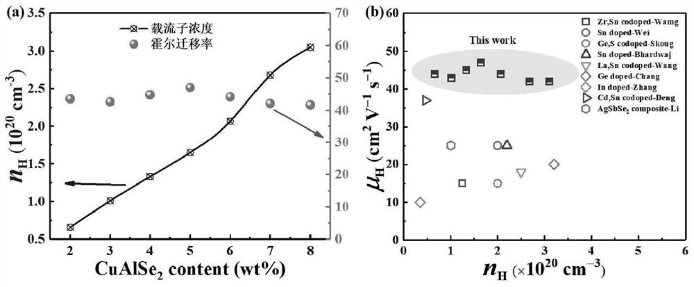
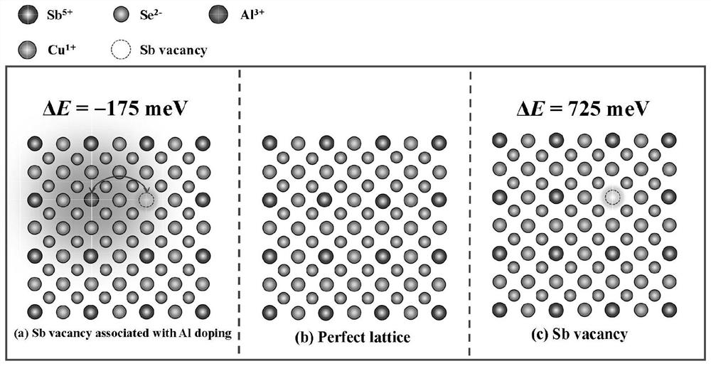
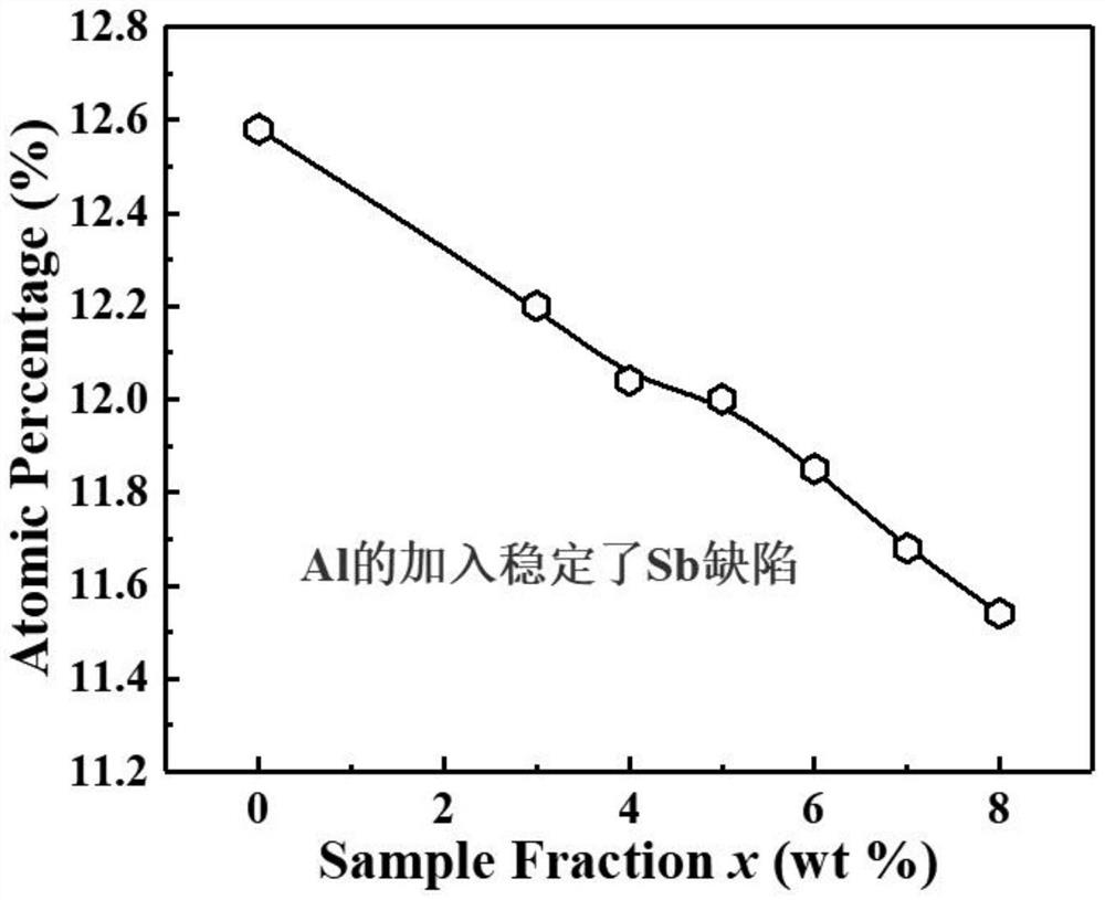
[0003] The invention provides an unconventional doping method for increasing the concentration of semiconductor carriers with high efficiency. The thermoelectric material Cu 3 SbSe 4 As an example, it solves the problems of low doping efficiency and poor conductivity of existing semiconductors

Method used


Image

  • Unconventional doping method for efficiently improving carrier concentration of semiconductor
  • Unconventional doping method for efficiently improving carrier concentration of semiconductor
  • Unconventional doping method for efficiently improving carrier concentration of semiconductor

Examples


Embodiment 1

[0029] An unconventional doping method for increasing the concentration of semiconductor carriers with high efficiency. The preparation steps are as follows: 3 Sb 1-δ Se 4 -x CuAlSe 2 (x=2wt%), accurately weigh raw materials in a glove box with an argon-protected environment, place in a quartz tube to vacuum seal the tube after weighing; the quartz tube with raw materials is placed in a horse-boiler, and the horse-boiler is heated at 5°C min -1 Slowly raise the temperature to 900°C, keep it warm for 12 hours, let the raw materials fully react, then take out the quartz tube, quench it in cold water and cool it quickly, then anneal at 450°C, pour the annealed sample into an agate grinding bowl, and grind it into powder carefully shape, and then made into a dense bulk material by hot pressing sintering technology.

Embodiment 2

[0031] An unconventional doping method for increasing the concentration of semiconductor carriers with high efficiency. The preparation steps are as follows: 3 Sb 1-δ Se 4 、CuAlSe 2 (x=3wt%), the raw materials were accurately weighed in a glove box with an argon-protected environment, and the rest of the operating steps were the same as in Example 1.

Embodiment 3

[0033] An unconventional doping method for increasing the concentration of semiconductor carriers with high efficiency. The preparation steps are as follows: 3 Sb 1-δ Se 4 、CuAlSe 2 (x=4wt%), the raw materials were accurately weighed in a glove box with an argon-protected environment, and the rest of the operating steps were the same as in Example 1.


PUM


Abstract

The invention discloses an unconventional doping method for efficiently improving the carrier concentration of a semiconductor, and relates to the technical field of semiconductors. The disclosed unconventional doping method for efficiently improving the carrier concentration of the semiconductor comprises the steps of: manufacturing vacancy defects of original elements of the semiconductor, and adding a small amount of heteroatoms (stable atoms) for stabilizing the defects; and accurately weighing raw materials in a glove box with an argon protection environment, putting the weighed raw materials into a quartz tube, sealing the quartz tube in vacuum, putting the quartz tube filled with the raw materials into a Muffle furnace, fully reacting, taking out the quartz tube, quenching in cold water, rapidly cooling, annealing at 450 DEG C, pouring into an agate grinding bowl for grinding, and then manufacturing a block material with good compactness through using a hot pressing sintering technology. According to the unconventional doping method, the semiconductor doping efficiency can be improved, the carrier mobility of the semiconductor is not damaged while the carrier concentration of the semiconductor is efficiently improved, and the electrical performance of the semiconductor is greatly improved.

Description

technical field [0001] The invention belongs to the technical field of semiconductors, and in particular relates to an unconventional doping method for increasing the concentration of semiconductor carriers with high efficiency. Background technique [0002] Doping semiconductors to improve their electrical conductivity is used as a key technology to adjust the electrical properties of semiconductor materials and devices. Semiconductor materials with excellent performance should maintain high mobility on the basis of optimizing carrier concentration. A common doping technique is to introduce heterogeneous elements into intrinsic semiconductors to provide carriers as acceptor impurities or donor impurities, and the carrier concentration will increase with the concentration of acceptor impurities and donor impurities. Because the doping of heteroatoms in the crystal is affected by many factors such as limited solubility, atomic radius and electronegativity difference, the eff...

Claims


Application Information

Patent Timeline
Patent Type & Authority Applications(China)
IPC IPC(8): H01L35/34H01L35/16H10N10/01H10N10/852
CPCH10N10/852H10N10/01
Inventor 卢旭周小元黄玉玲张斌王桂文
Owner CHONGQING UNIV
Learn More