

A method for preparing metal quasi-nano-lattice and the product obtained
A nanocrystal, gold standard technology, applied in the field of materials, can solve the problems of limiting the multi-functional application of nanolattice materials, material selection limitations, low nanolattice efficiency, etc., to achieve excellent mechanical properties and energy absorption capacity, material types The effect of large selection and uniform feature size selection range
- Summary
- Abstract
- Description
- Claims
- Application Information
AI Technical Summary
Problems solved by technology
Method used
Image

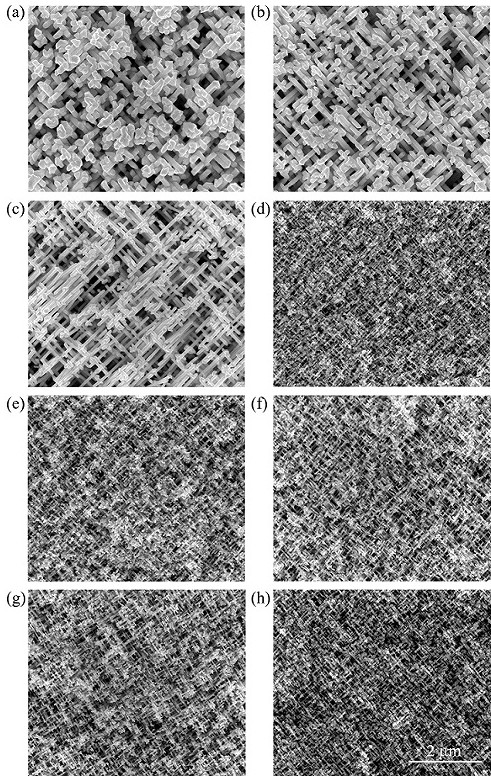
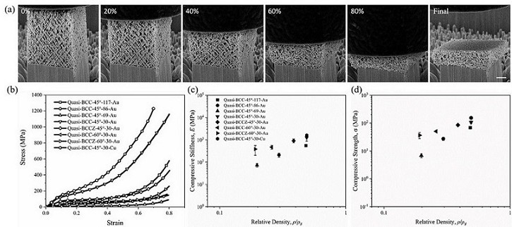
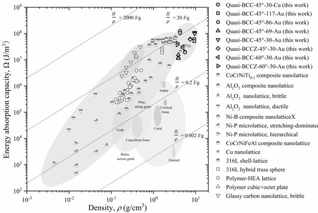
Examples
Embodiment 1
[0045] Embodiment 1, the preparation method of the gold quasi-nano-lattice with 117 ± 4 nm feature size
[0046] The method for preparing the gold quasi-nano-lattice with 117 ± 4 nm characteristic size provided by the present invention comprises the following steps:
[0047] 1) Ta ion irradiation was carried out on a polycarbonate (PC) film with a thickness of 30 μm. During irradiation, the angle between the ion beam and the film plane was 45°, and the irradiation fluence was 1×10 9 ×4ions / cm 2 (i.e., irradiate 4 times, each time 1×10 9 ions / cm 2 ) to obtain an ion track film irradiated by heavy ions;
[0048] 2) UV light sensitization on both sides of the obtained PC ion tracker film irradiated by heavy ions for 2 hours each;
[0049]3) Put the sensitized PC ion track film into 50℃, 5mol / L NaOH solution for chemical etching for 5min40s;
[0050] 4) Sputter a layer of gold with a thickness of about 20nm on one side of the etched polymer film;
[0051] 5) Electrochemical...
Embodiment 2
[0054] Embodiment 2, the preparation method of the gold quasi-nano-lattice with 86 ± 4 nm feature size
[0055] The method for preparing the gold quasi-nano lattice with 86 ± 4 nm characteristic size provided by the present invention comprises the following steps:
[0056] 1) See step 1 of Example 1);
[0057] 2) See step 2 of Example 1);
[0058] 3) Put the sensitized PC ion track film into 50℃, 5mol / L NaOH solution for chemical etching for 3min57s;
[0059] 4) See step 4 of Example 1);
[0060] 5) Electrochemical deposition of copper substrate on the gold-sprayed side of the gold-sprayed polymer film, the composition of the copper electrolyte used is 75g / l Cu 2 SO 4 ·5H 2 O+30 g / l H 2 SO 4 , the deposition voltage is 0.5V, and the deposition time is 1h; on the other side, metal gold is electrochemically deposited, and the composition of the gold electrolyte used is 75 g / l Na 3 Au(SO 3 ) 2 , the deposition voltage is 1.3 V, 15 s; -0.25 V, 5 s pulse electrodeposition...
Embodiment 3
[0063] Embodiment 3, the preparation method of the gold quasi-nano-lattice with 69 ± 4 nm feature size
[0064] The method for preparing a gold quasi-nano-lattice with a characteristic size of 69 ± 4 nm provided by the present invention comprises the following steps:
[0065] 1) See step 1 of Example 1);
[0066] 2) See step 2 of Example 1);
[0067] 3) Put the sensitized PC ion track film into 50℃, 5mol / L NaOH solution for chemical etching for 2min36s;
[0068] 4) See step 4 of Example 1);
[0069] 5) Electrochemical deposition of copper substrate on the gold-sprayed side of the gold-sprayed polymer film, the composition of the copper electrolyte used is 75g / l Cu 2 SO 4 ·5H 2 O+30 g / l H 2 SO 4 , the deposition voltage is 0.5V, and the deposition time is 1h; on the other side, metal gold is electrochemically deposited, and the composition of the gold electrolyte used is 75 g / l Na 3 Au(SO 3 ) 2 , the deposition voltage is 1.3 V, 15 s; -0.25 V, 5 s pulse electrodeposit...
PUM
| Property | Measurement | Unit |
|---|---|---|
| size | aaaaa | aaaaa |
| compressive yield strength | aaaaa | aaaaa |
| size | aaaaa | aaaaa |
Abstract
Description
Claims
Application Information