Novel patterned electrode preparation method
A technology for preparing electrodes and patterning, which is applied in the direction of circuits, electrical components, semiconductor devices, etc., can solve the problems of high time cost and economic cost, complex process, and low production capacity, so as to improve the efficiency of electrode patterning and increase adhesion , the effect of improving reliability
- Summary
- Abstract
- Description
- Claims
- Application Information
AI Technical Summary
Problems solved by technology
Method used
Image

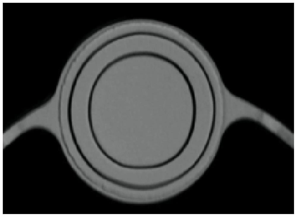
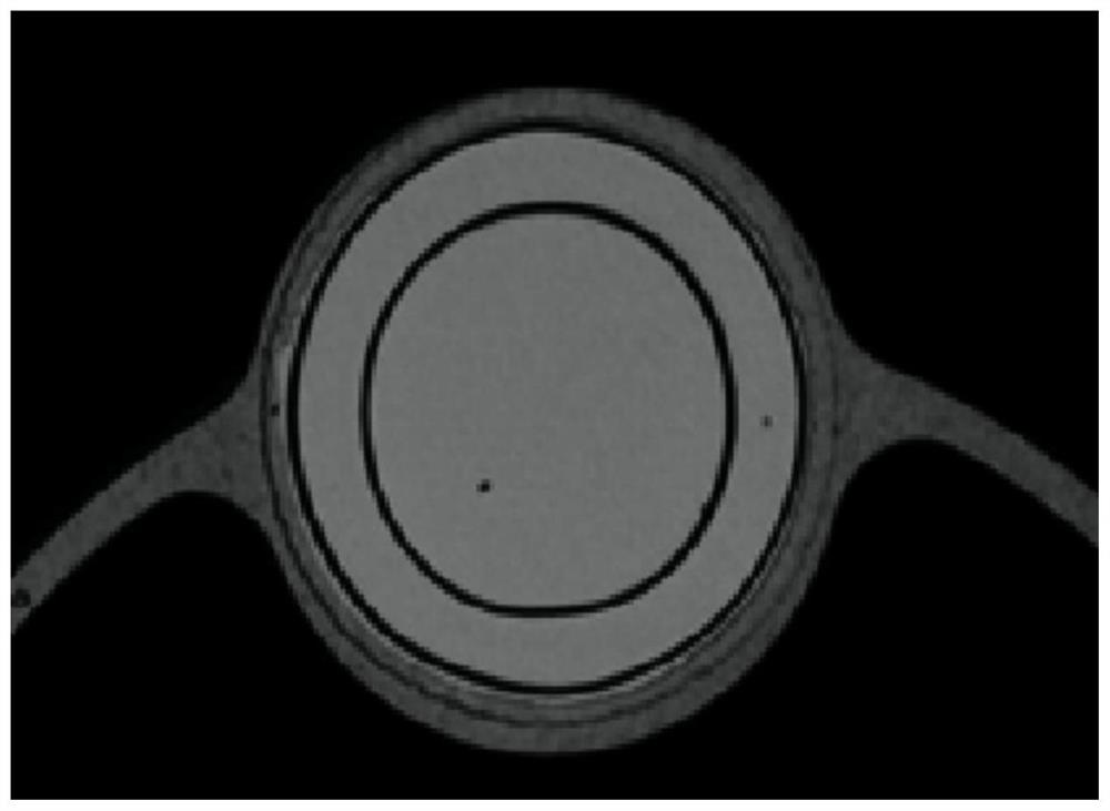
Examples
Embodiment Construction
[0030] The technical solutions in the embodiments of the present invention will be clearly and completely described below in conjunction with the accompanying drawings in the embodiments of the present invention. Obviously, the described embodiments are only some, not all, embodiments of the present invention. Based on the embodiments of the present invention, all other embodiments obtained by persons of ordinary skill in the art without creative efforts fall within the protection scope of the present invention.
[0031] In order to solve the problems of the current traditional electrode patterning method with many steps in the preparation process, low fault tolerance, complex process and low production capacity, and high time and economic costs, this application provides a new method for preparing electrode patterning.
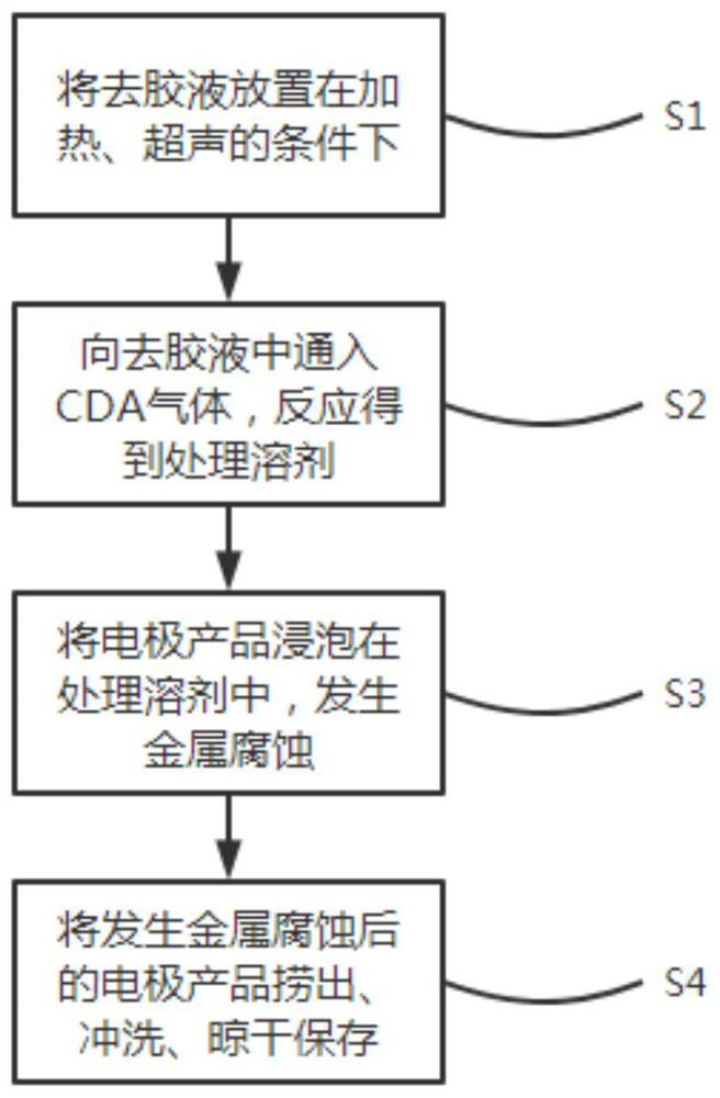
[0032] see figure 1 , is a flowchart of an embodiment of a novel method for preparing electrode patterning.
[0033] As can be seen from the figure, the pre...
PUM
 Abstract
Description
Claims
Application Information