Superconducting quantum chip and preparation method and application thereof

A superconducting quantum and chip technology, applied in the manufacture/processing of superconducting devices, superconducting devices, superconducting components, etc., can solve the problems of limiting the development of superconducting quantum chips and the inability to increase the number of qubits in quantum chips, etc. The effect of increasing the number of qubits

Pending Publication Date: 2022-03-11
北京量子信息科学研究院
View PDF0 Cites 0 Cited by
  • Summary
  • Abstract
  • Description
  • Claims
  • Application Information

AI Technical Summary

Problems solved by technology

However, the air bridge structure can only suppress the interference between microwave signals, and cannot increase the number of qubits in quantum chips, which limits the development of superconducting quantum chips

Method used


Image

  • Superconducting quantum chip and preparation method and application thereof
  • Superconducting quantum chip and preparation method and application thereof

Examples


preparation example Construction

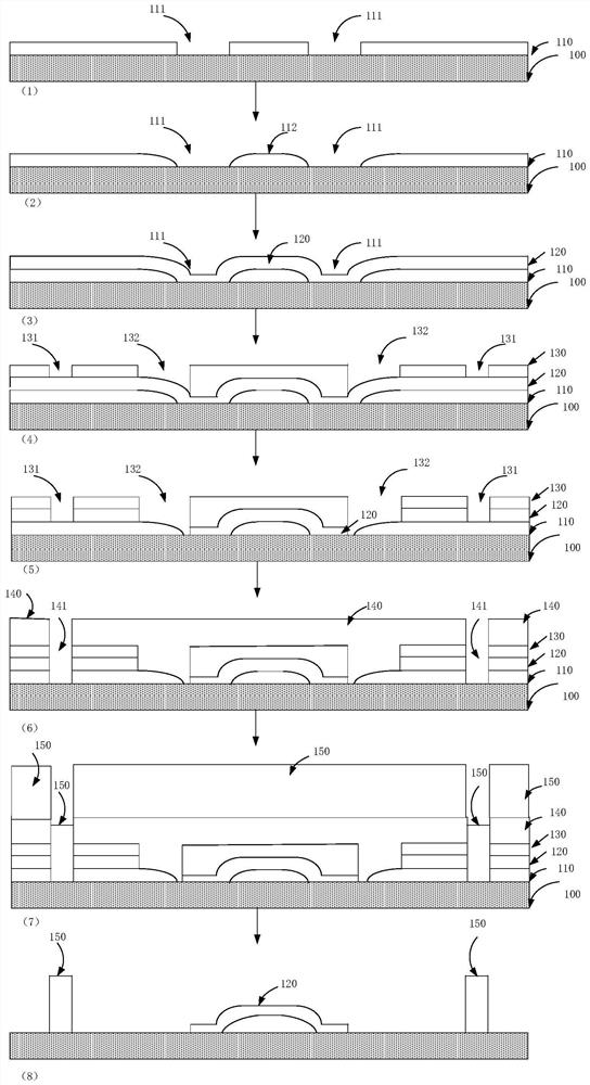
[0037] see figure 1 , the embodiment of the present invention provides a method for preparing a superconducting quantum chip, comprising the following steps:

[0038]Step S10, providing a substrate provided with a circuit, and forming a first photoresist layer having two grooves arranged at intervals on the substrate, where the grooves are located as pier regions, and the two grooves are The first photoresist layer between the grooves acts as a bridge support;

[0039] Step S20, forming a first metal film layer on the first photoresist layer;

[0040] Step S30, covering and forming a second photoresist layer on the first metal film layer, and defining a first metal column area and a separation groove area on the second photoresist layer, and the separation groove area and the bridge pier areas are connected and located on the side of the pier area away from the bridge support body, and the first metal column area is located on the side of the separation groove area away from...

Embodiment 1

[0083] see figure 2 , the preparation method of the superconducting quantum chip is as follows:

[0084] A single crystal silicon wafer is used as a substrate, and a superconducting circuit structure is fabricated on the substrate to obtain a substrate 100 provided with circuits. The superconducting circuit structure can be provided, fabricated or formed using techniques known in the art.

[0085] (1) Form a layer of photoresist on the substrate 100 provided with the circuit, and form two grooves arranged at intervals in the photoresist to define the bridge pier region 111 to obtain the first photoresist layer 110 . The groove is the pier area 111 of the air bridge.

[0086] Specific method: use a spin coater to spin coat LOR 10B glue on the above-mentioned substrate 100 provided with a circuit, the spin coating speed is 2000 rpm, and the spin coating time is 60 sec. Use a hot plate to bake the substrate spin-coated with LOR 10B glue at 200°C for 10 minutes.

[0087] Afte...

Embodiment 2

[0106] see also figure 2 , the preparation method of the superconducting quantum chip is as follows:

[0107] A single crystal silicon wafer is used as the substrate 100, and a layer of superconducting metal film has been covered on the surface of the substrate. A superconducting circuit structure is fabricated on the substrate to obtain a substrate 100 provided with circuits. The superconducting circuit structure can be provided, fabricated or formed using techniques known in the art.

[0108] (1) Form a layer of photoresist on the substrate 100 provided with the circuit, and form two grooves arranged at intervals in the photoresist to define the bridge pier region 111 to obtain the first photoresist layer 110 . The groove is the pier area 111 of the air bridge.

[0109] Specific method: Spin-coat S1813 photoresist on the substrate in step 1 at a rotation speed of 800 rpm, and bake on a hot plate at 115° C. for 2 minutes after the coating is completed.

[0110] The pier ...


PUM

PropertyMeasurementUnit
Thicknessaaaaaaaaaa
Thicknessaaaaaaaaaa
Outer diameteraaaaaaaaaa

Abstract

The invention relates to the technical field of micro-nano processing, in particular to a superconducting quantum chip and a preparation method and application thereof. The preparation method of the superconducting quantum chip comprises the following steps that a substrate provided with a circuit is provided, a first photoresist layer with two grooves arranged in a spaced mode is formed on the substrate, and the portion, between the two grooves, of the first photoresist layer serves as a bridge supporting body; forming a first metal film layer on the first photoresist layer; forming a second photoresist layer on the first metal film layer in a covering manner, and defining a first metal column region and a separation groove region on the second photoresist layer; removing the second photoresist layer and the first metal film layer in the first metal column region and the separation groove region; covering the second photoresist layer to form a third photoresist layer, and etching to expose the substrate and form a second metal column region; forming a second metal film layer on the third photoresist layer and the second metal column region; and removing each photoresist layer.

Description

technical field [0001] The invention relates to the technical field of micro-nano processing, in particular to a superconducting quantum chip and its preparation method and application. Background technique [0002] Compared with traditional computers, superconducting quantum computers have superior computing power and become a research hotspot in the world. Superconducting quantum chips with superconducting microwave circuit systems are by far the most promising system chips for realizing universal quantum computing. Universal fault-tolerant quantum computing requires tens of thousands or even millions of physical qubits. With the help of the compatibility of traditional semiconductor processes, the use of micro-nano processing technology to prepare superconducting microwave circuit systems can continuously meet the expansion requirements of quantum chips. [0003] Controlling qubits on a superconducting quantum chip with a superconducting microwave circuit system requires ...

Claims


Application Information

Patent Timeline
IPC IPC(8): H01L39/24H01L39/22H01L39/02
CPCH10N60/805H10N60/12H10N60/0912
Inventor 王光月杨楚宏李成垚金贻荣
Owner 北京量子信息科学研究院
Why Eureka
Try Eureka