Optical film with high hardness, strong adhesive force and anti-wear function
An optical film, strong adhesion technology, applied in optics, optical components, instruments, etc., can solve the problems of easy cracking of the film, high film stress, poor friction resistance, etc., to achieve high film adhesion and reduce dirt. Residue, excellent scratch and dirt resistance
- Summary
- Abstract
- Description
- Claims
- Application Information
AI Technical Summary
Problems solved by technology
Method used
Image
Examples
Embodiment 2
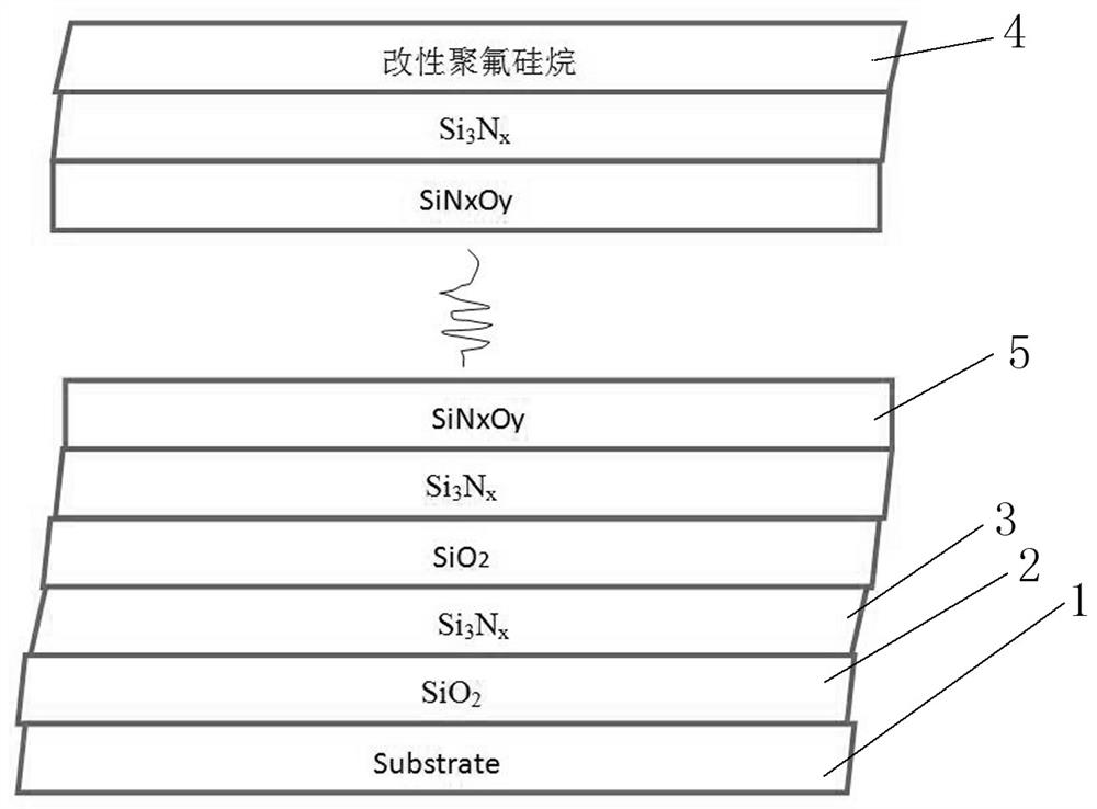
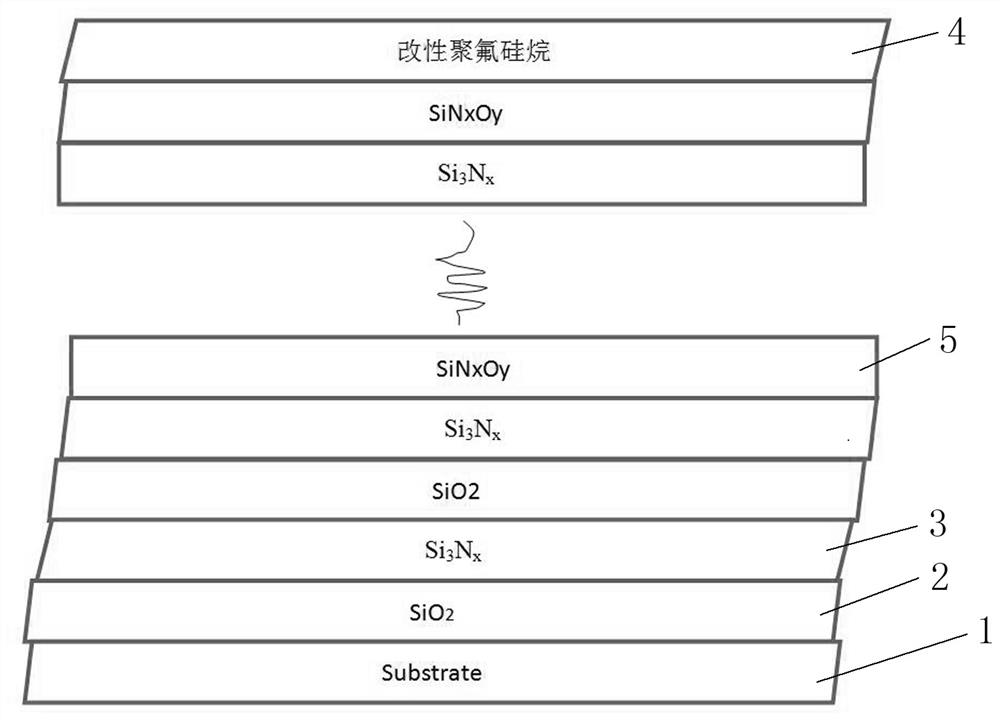
[0039] Embodiment 2, as attached figure 2 As shown, the superhard anti-reflection film is coated on the glass substrate, and the material of the film system is SiO 2 、Si 3 N x and SiN x o y One or more of them are stacked or staggered. The reference wavelength of the film system is λc=550nm, and there are 8 layers in total including the modified polyfluorosilane layer. During the specific production, the anti-reflection layer formed in the optical coating, the optical function Layer or decorative functional layer is made of Si, SiO 2 、Si 3 N x and SiN x o y One or more of them are alternately plated in 7 layers, and then thermally evaporated or sprayed with modified polyfluorosilane to form a waterproof and oil-proof functional layer on the film layer. The layout and physical thickness of each layer of the film system in this embodiment are shown in the table 2:
[0040] .
[0041] The wear resistance of the optical film in Example 2 is checked by the steel wool ...
Embodiment 3
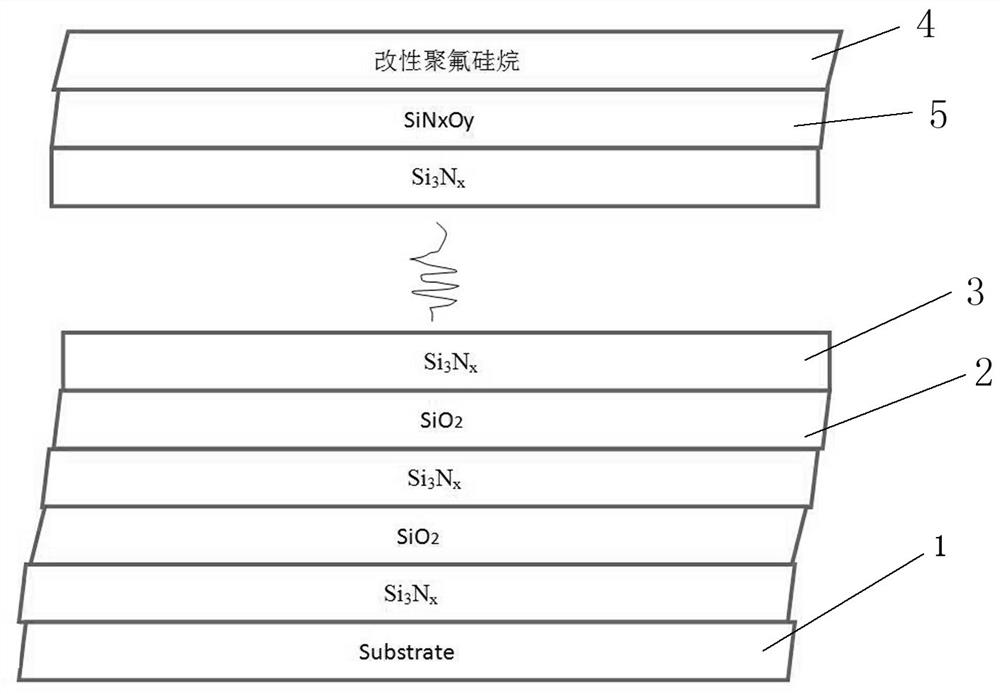
[0050] Embodiment 3, as attached image 3 As shown, the superhard anti-reflection film is coated on the glass substrate, and the material of the film system is SiO 2 、Si 3 N x and SiN x o y One or more of them are stacked or staggered. The reference wavelength of the film system is λc=550nm, and there are 9 layers in total including the modified polyfluorosilane layer. During specific production, the anti-reflective layer formed in the optical coating, the optical function Layer or decorative functional layer is made of Si, SiO 2 、Si 3 N x and SiN x o y One or more of them are alternately plated in 8 layers, and the modified polyfluorosilane is plated on the film layer by thermal evaporation or spraying. The layout and physical thickness of each layer of the film system in this embodiment are shown in Table 3:
[0051] .
[0052] Check the wear resistance of the optical film in embodiment 3 by the vibration friction test method:
[0053] 1) Using the German Rosler...
PUM
| Property | Measurement | Unit |
|---|---|---|
| thickness | aaaaa | aaaaa |
| hardness | aaaaa | aaaaa |
| thickness | aaaaa | aaaaa |
Abstract
Description
Claims
Application Information


