Super-radiation light-emitting diode chip integrated with lateral detector and preparation method of super-radiation light-emitting diode chip

A technology of superluminescent light-emitting diodes, which is applied in the direction of semiconductor devices, final product manufacturing, sustainable manufacturing/processing, etc., and can solve problems such as increased ripple coefficient of superluminescent light-emitting diodes, enhanced chip reflectivity, and unfavorable weak light detection. , to achieve the effects of low-light detection, improvement of ripple coefficient, and avoiding the increase of ripple coefficient

Pending Publication Date: 2022-03-18
THE 44TH INST OF CHINA ELECTRONICS TECH GROUP CORP +2
View PDF0 Cites 0 Cited by
  • Summary
  • Abstract
  • Description
  • Claims
  • Application Information

AI Technical Summary

Problems solved by technology

[0004] In view of this, the purpose of the present invention is to provide a superluminescent light-emitting diode chip with integrated side detectors and its preparation method, to solve the problems caused by the introduction of isolation grooves in the prior art when the detector and the superluminescent light-emitting diode chip are integrated. Increased reflectivity at the back end of the chip, leading to increased ripple factor of superluminescent light-emitting diodes, and problems that are not conducive to low-light detection

Method used


Image

  • Super-radiation light-emitting diode chip integrated with lateral detector and preparation method of super-radiation light-emitting diode chip
  • Super-radiation light-emitting diode chip integrated with lateral detector and preparation method of super-radiation light-emitting diode chip
  • Super-radiation light-emitting diode chip integrated with lateral detector and preparation method of super-radiation light-emitting diode chip

Examples


Embodiment 1

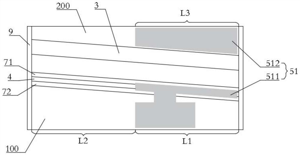
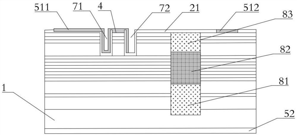
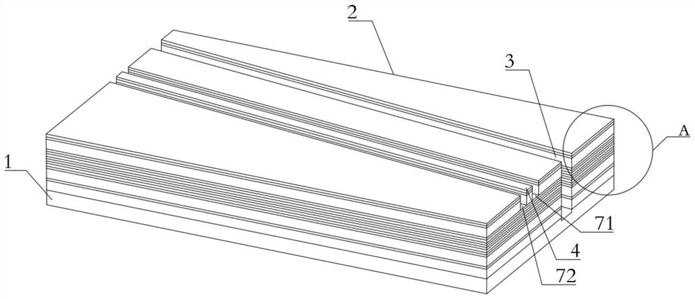
[0040] Such as figure 1 Shown is a schematic structural view of a superluminescent light-emitting diode chip integrated with a lateral detector according to Embodiment 1 of the present invention. The superluminescent light emitting diode chip with integrated lateral detector in this embodiment includes a superluminescent light emitting diode 100 and a lateral detector 200 integrated on the same chip. Specifically, this embodiment includes a substrate 1 and a substrate 1 formed on the same chip. The epitaxial wafer 2 on the substrate 1, the upper surface of the epitaxial wafer 2 is formed with an isolation groove 3 penetrating the epitaxial wafer 2 downward, and the isolation groove 3 can separate the epitaxial wafer 2 into an independent first part and The second part, the first part is used to form the SLED 100 , and the second part is used to form the lateral detector 200 . Specifically, the upper surface of the epitaxial wafer 2 of the first part is formed with a ridge waveg...

Embodiment 2

[0048] Such as Figure 5 Shown is a flow chart of a method for preparing a superluminescent light emitting diode chip integrated with a lateral detector in embodiment 2 of the present invention, which is used to prepare the superluminescent light emitting diode chip integrated with a lateral detector in embodiment 1. This embodiment specifically includes the following steps:

[0049] S100: Provide a substrate 1, and grow an epitaxial wafer 2 on the substrate 1.

[0050] Specifically, an n-InP substrate 1 is provided, and an n-InP buffer layer 201, an n-InGaAsP extended waveguide layer 202, an n-InP spacer layer 203, and an n-AlGaInAs transition layer are sequentially grown on the InP substrate 1. layer 204, n-AlInAs lower confinement layer 205, i-AlGaInAs lower waveguide layer 206, AlGaInAs active layer 207, i-AlGaInAs upper waveguide layer 208, p-AlInAs first upper confinement layer 209, p-InP second upper limit Value layer 210, p-InGaAsP etch stop layer 211, p-InP third up...


PUM

PropertyMeasurementUnit
Widthaaaaaaaaaa

Abstract

The invention discloses a super-radiation light-emitting diode chip integrated with a lateral detector and a preparation method, the super-radiation light-emitting diode chip comprises a substrate and an epitaxial wafer formed on the substrate, and an isolation groove penetrating through the epitaxial wafer downwards is formed in the upper surface of the epitaxial wafer. A ridge waveguide arranged in parallel with the isolation groove is formed on one side, corresponding to the isolation groove, of the upper surface of the epitaxial wafer, and an active area and a passive absorption area are sequentially formed on the side in the length direction of the ridge waveguide. A lateral detection area is formed on the other side, corresponding to the isolation groove, of the epitaxial wafer and at the position opposite to the active area, the ripple coefficient of the super-radiation light-emitting diode can be effectively improved, and the influence of introduction of a passive absorption area on the light detection capacity of a lateral detector is reduced.

Description

technical field [0001] The invention relates to the technical field of superluminescent light emitting diodes, in particular to a superluminescent light emitting diode chip integrated with a lateral detector and a preparation method thereof. Background technique [0002] Superluminescent light-emitting diode light source is a semiconductor superluminescent light-emitting diode that combines the advantages of LD and LED. It has the advantages of high brightness, wide spectrum, short coherence, low intensity noise and high efficiency. It is widely used in all solid-state fiber optic gyroscopes, optical Communication, optical information processing, biomedical optical coherence test technology and other optical sensing and optical communication fields have broad military and civilian application prospects. Since the output optical power of the superluminescent light-emitting diode chip has a phenomenon of slow decay during long-term use, its power needs to be monitored. Usually...

Claims


Application Information

Patent Timeline
IPC IPC(8): H01L31/0232H01L31/0352H01L31/12H01L31/18H01L33/00H01L33/20
CPCH01L33/20H01L33/0062H01L31/125H01L31/1844H01L31/035272H01L31/02327Y02P70/50
Inventor 周帅庞福滨张靖袁宇波田坤嵇建飞刘海军许瑨
Owner THE 44TH INST OF CHINA ELECTRONICS TECH GROUP CORP
Why Eureka
Try Eureka