Supercharge Your Innovation With Domain-Expert AI Agents!

Electrostatic protection device

An electrostatic protection and device technology, applied in the field of electrostatic protection devices, can solve problems such as latch-up effects that are prone to occur, reduce the risk of latch-up effects, and increase the effect of maintaining voltage

Pending Publication Date: 2022-03-25
SHANGHAI HUAHONG GRACE SEMICON MFG CORP
View PDF0 Cites 0 Cited by
  • Summary
  • Abstract
  • Description
  • Claims
  • Application Information

AI Technical Summary

Problems solved by technology

However, the maintenance voltage (Vh) of pure SCR structure after snapback (snapback) generally does not exceed 10V, and there is a greater risk of latchup in high-voltage port applications, that is, when the power supply voltage of the high-voltage port is greater than the SCR maintenance Latch-up effect is prone to occur when the voltage

Method used


Image

  • Electrostatic protection device
  • Electrostatic protection device
  • Electrostatic protection device

Examples


Embodiment Construction

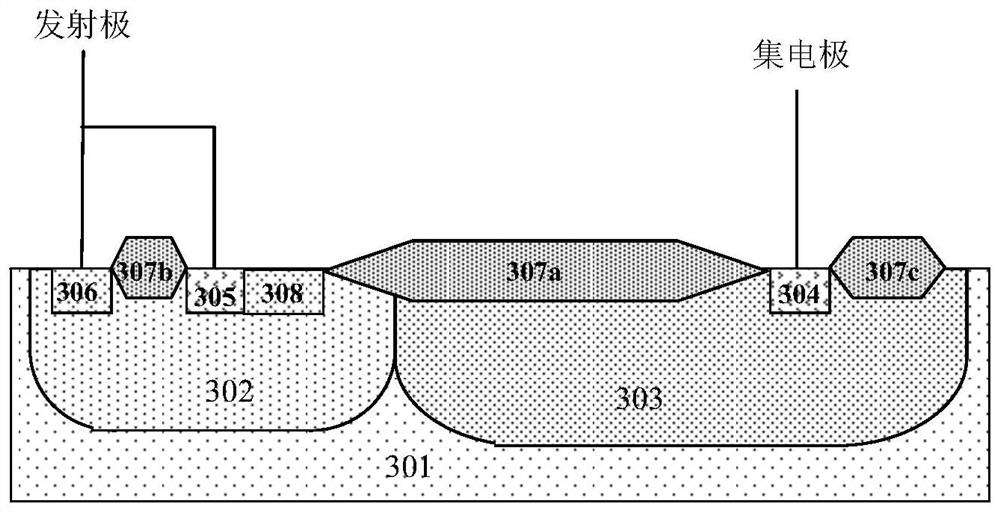
[0058] Such as image 3 Shown is a schematic cross-sectional structure diagram of the electrostatic protection device of the first embodiment of the present invention; Figure 4 Shown is the layout of the electrostatic protection device of the first embodiment of the present invention; the electrostatic protection device of the embodiment of the present invention is formed by a triode, and the triode includes:

[0059] A first high-voltage well region 302 doped with a second conductivity type, and a second high-voltage well region 303 doped with a first conductivity type; both the first high-voltage well region 302 and the second high-voltage well region 303 are formed in In the semiconductor substrate 301 .

[0060] In the first embodiment of the present invention, the semiconductor substrate 301 includes a silicon substrate. The semiconductor substrate 301 is P-type doped. In other embodiments, it can also be: the semiconductor substrate 301 is N-type doped.

[0061] In ...


PUM


Abstract

The invention discloses an electrostatic protection device, which is formed by a triode and comprises a first high-voltage well region doped with a second conductive type and a second high-voltage well region doped with a first conductive type, a first conductive type heavily doped first diffusion region is formed in the second high-voltage well region; a first conductive type heavily doped second diffusion region is formed in the first high-voltage well region, and the first diffusion region and the second high-voltage well region form a collector region; the second diffusion region forms an emitter region; the first high-voltage well region forms a base region; a heavily doped third diffusion region of the second conductive type is formed outside the first side surface of the second diffusion region; a second conductive type heavily doped fourth diffusion region is formed in the surface region of the first high-voltage well region outside the second side surface of the second diffusion region; the second and third diffusion regions are both connected to the emitter; the first diffusion region is connected to the collector; the fourth diffusion region is floating. According to the invention, the sustaining voltage after the snapback of the triode can be improved.

Description

technical field [0001] The invention relates to a semiconductor integrated circuit, in particular to an electrostatic protection (ESD) device. Background technique [0002] Such as figure 1 Shown is the application circuit diagram of the electrostatic protection device; the electrostatic protection device 102 is arranged between the input and output pads 101 and the ground, and when static electricity appears in the input and output pads 101, the electrostatic protection device 102 is triggered and discharges the static electricity, Thus, the protection of the internal circuit 103 is realized. [0003] Such as figure 2 As shown, it is a schematic cross-sectional structure diagram of an existing electrostatic protection device; the existing electrostatic protection device 102 is formed by a triode, and the triode includes: [0004] A first high-voltage well region 202 doped with a second conductivity type, and a second high-voltage well region 203 doped with a first condu...

Claims


Application Information

Patent Timeline
IPC IPC(8): H01L29/06H01L29/08H01L29/10H01L27/02
CPCH01L29/0808H01L29/1008H01L29/0615H01L29/0684H01L27/0259
Inventor 苏庆
Owner SHANGHAI HUAHONG GRACE SEMICON MFG CORP
Features
  • R&D
  • Intellectual Property
  • Life Sciences
  • Materials
  • Tech Scout
  • Unparalleled Data Quality
  • Higher Quality Content
  • 60% Fewer Hallucinations
Learn More