Micro light-emitting chip assembly and manufacturing method thereof, and micro light-emitting chip transfer method

A technology of light-emitting chips and manufacturing methods, which is applied in the fields of semiconductor/solid-state device manufacturing, electrical components, and electric-solid-state devices, etc., can solve the problems of complex transfer process, low transfer success rate, low efficiency, etc.

Active Publication Date: 2022-03-29
CHONGQING KONKA PHOTOELECTRIC TECH RES INST CO LTD
View PDF6 Cites 0 Cited by
  • Summary
  • Abstract
  • Description
  • Claims
  • Application Information

AI Technical Summary

Problems solved by technology

[0005] In view of the deficiencies of the above-mentioned related technologies, the purpose of this application is to provide a micro-light-emitting chip assembly and its manufacturing method, and a micro-light-emitting chip transfer method, aiming to solve the problem of low transfer success rate and relatively low transfer process in the transfer of LED chips in the related technology. Complex, Inefficient Problems

Method used


Image

  • Micro light-emitting chip assembly and manufacturing method thereof, and micro light-emitting chip transfer method
  • Micro light-emitting chip assembly and manufacturing method thereof, and micro light-emitting chip transfer method
  • Micro light-emitting chip assembly and manufacturing method thereof, and micro light-emitting chip transfer method

Examples


application example 1

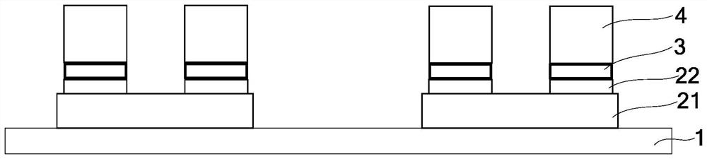
[0105] Please refer to Figure 10-1 to Figure 10-2 shown, including but not limited to:

[0106] S1001: Provide a first substrate 1 on which micro light-emitting chips are grown.

[0107] In this application example, the epitaxial layer 21 can be grown epitaxially on the first substrate 1 , and then the electrode 22 can be fabricated on the epitaxial layer.

[0108] S1002: Form independent thin film layers 3 on the electrodes of the micro light-emitting chips on the first substrate 1 respectively.

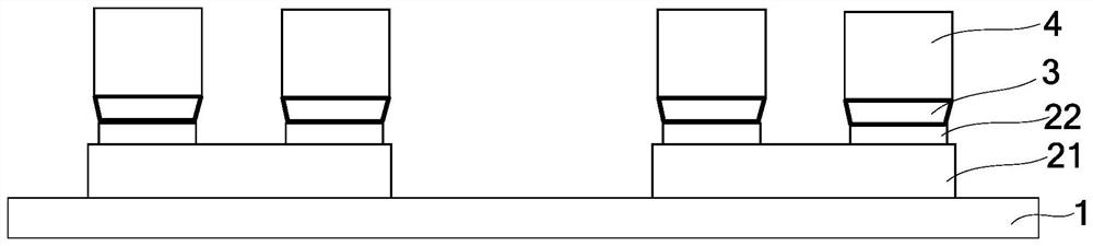
[0109] In this embodiment, the form of each micro light emitting chip on the first substrate 1 is that the electrode of each micro light emitting chip is exposed upward, and a layer of lithium fluoride thin film is formed on the electrode 22 of each micro light emitting chip by evaporation. Layer 3 has water-swelling characteristics, that is, the film thin layer will swell after absorbing water, so that the contact surface of the surface in contact with it becomes smaller.

[01...

application example 2

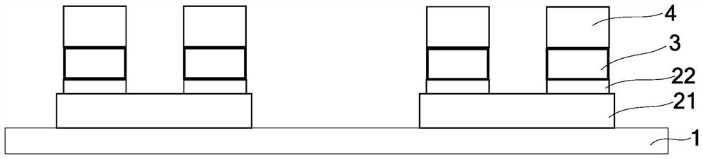
[0133] Please refer to Figure 11-1 to Figure 11-2 shown, including but not limited to:

[0134] S1101: Provide a first substrate 1 on which micro light-emitting chips are grown.

[0135] In this application example, the epitaxial layer 21 can be grown epitaxially on the first substrate 1 , and then the electrode 22 can be fabricated on the epitaxial layer.

[0136] S1102: Form independent thin film layers 3 on the electrodes of the micro light-emitting chips on the first substrate 1 respectively.

[0137] In this embodiment, the form of each micro light emitting chip on the first substrate 1 is that the electrode of each micro light emitting chip is exposed upward, and a layer of organic porous material is formed on the electrode 22 of each micro light emitting chip by evaporation. The thin film layer 3 has the property of swelling upon water absorption, that is, the thin film layer swells after absorbing water, so that the contact surface of the surface in contact with it ...


PUM


Abstract

The invention relates to a micro light-emitting chip assembly, a manufacturing method thereof and a micro light-emitting chip transfer method. A water-swellable thin film layer and a support body for increasing the epitaxial height of each electrode are sequentially formed on the electrode of each micro light-emitting chip, so that the electrode of each micro light-emitting chip can be reliably connected with an adhesive layer by means of the thin film layer and the support body in the chip transfer process, and the chip transfer reliability and success rate are improved; after the thin film layers absorb water and expand, the contact area between the thin film layers and the electrodes becomes smaller to form a weakening structure, so that the picked electrodes of the micro light-emitting chip can be directly separated from the thin film layers, the step of carrying out debonding treatment on the adhesive layers in a light or heat mode can be omitted, the micro light-emitting chip transfer process is simplified, and the production efficiency is improved. And the convenience and the efficiency of transferring the micro light-emitting chip are improved, the manufacturing period of the display backboard can be shortened, and the manufacturing cost is reduced.

Description

technical field [0001] The invention relates to the field of semiconductor devices, in particular to a micro-light-emitting chip assembly, a manufacturing method thereof, and a micro-light-emitting chip transfer method. Background technique [0002] At present, a key technology facing micro-LED (micro-Light Emitting Diode, miniature light-emitting diode) is to transfer the micro-LED chip to the display backplane through mass transfer. In related technologies, a detachable adhesive layer is generally provided on the first temporary substrate, and the micro-LED chip is transferred from the growth substrate to the first temporary substrate by adhesion through the detachable adhesive layer, and then the second temporary substrate is used. The second temporary substrate transfers the micro-LED chips from the first temporary substrate to the display backplane. In this process, the thickness of the glue layer set on the first temporary substrate often has uneven thickness, resulti...

Claims


Application Information

Patent Timeline
Patent Type & Authority Applications(China)
IPC IPC(8): H01L33/44H01L33/00H01L21/683
CPCH01L33/44H01L33/005H01L21/6835H01L2933/0025H01L2221/68381H01L2221/68386H01L2221/68368
Inventor 蒲洋洪温振
Owner CHONGQING KONKA PHOTOELECTRIC TECH RES INST CO LTD
Why Eureka
Try Eureka