
Light-emitting element

A light-emitting element and cladding layer technology, which is applied in the direction of electrical components, semiconductor devices, circuits, etc., can solve the problems of lateral diffusion, the inability to increase the total luminous energy, and cumbersome procedures, etc., and achieve the effect of increasing the total luminous energy

Pending Publication Date: 2022-04-15
兆劲科技股份有限公司
View PDF0 Cites 0 Cited by
  • Summary
  • Abstract
  • Description
  • Claims
  • Application Information

AI Technical Summary

Problems solved by technology

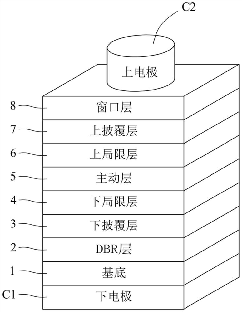
However, such a structural design is only suitable for low current (for example, less than 8mA (milliampere)) operating conditions, because the lower current allows carriers to have enough time to diffuse laterally in the window layer 8
[0004] When in order to increase the total power of LED light emission, it is usually input from the upper electrode C2 by increasing the current (for example, greater than or equal to 8mA). Diffusion, that is to say, compared with low current, the carrier is more confined under the circular area under the operating condition of high current, so the carrier density under the circular area is higher, even if the window layer 8 No matter how thick the thickness is, it will not be able to spread the high current laterally in time
The aforesaid high current cannot be diffused laterally in time, resulting in only a part of the quantum well structure of the active layer 15 being used. In addition, the higher carrier density under the aforementioned circular area also causes the temperature of the active layer 5 to be higher during LED operation, for example, as high as 485°C (at a high current of 10mA), however, the higher temperature of the active layer will make the total luminous energy of the LED unable to effectively increase with the increase of the current
[0005] Furthermore, as mentioned above, the upper electrode C2 must be made by etching, which makes it necessary to go through epitaxy and etching processes when making LEDs. Therefore, the manufacturing process is cumbersome, the risk is also increased, and the yield is facing challenges.

Method used


Image

  • Light-emitting element
  • Light-emitting element
  • Light-emitting element

Examples


Embodiment 1

[0032]

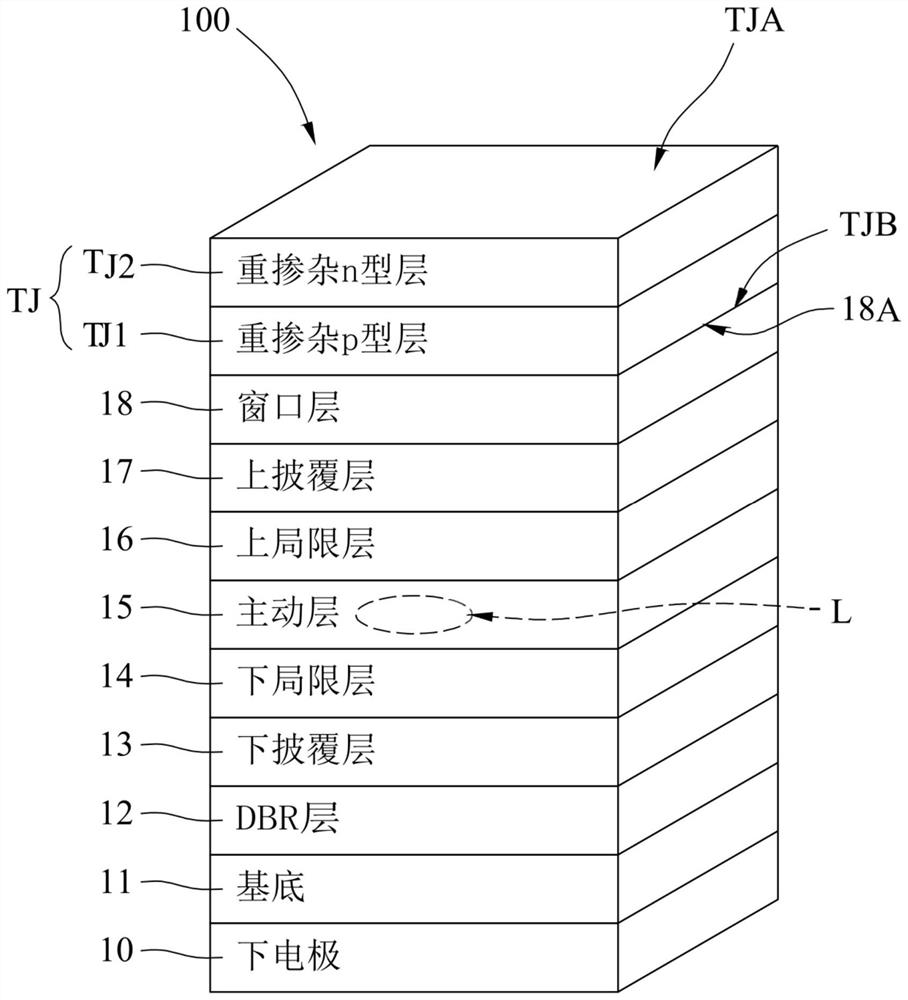
[0033] *: The area of ​​the upper surface TJA and the area of ​​the lower surface TJB of the tunnel junction layer TJ are respectively equal to the area of ​​the window layer upper surface 18A of the window layer 18 .

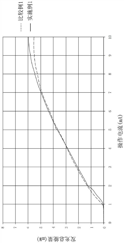
[0034] Table 3 below lists the total luminous energy of Example 1 and Comparative Example 1 of the light-emitting element 100 of the present invention under high current (greater than or equal to 8mA) operating conditions. Also see image 3 .

[0035] Table three

[0036]

[0037] Table 4 below lists the temperatures of the active layer 15 of Example 1 of the light-emitting element 100 of the present invention and the active layer of Comparative Example 1 under the operating condition of an operating current of 10 mA.

[0038] Table four

[0039] Operating current 10mA Active layer (E) of Comparative Example 1 485℃ Active layer 15(F) of embodiment 1 390℃ (F)-(E) -95℃

[0040] It can be seen from the above Tab...


PUM


Abstract

The invention provides a light-emitting element. The light-emitting element comprises a substrate, a lower cladding layer, a lower confinement layer, an active layer, an upper confinement layer, an upper cladding layer, a window layer and a tunnel junction layer which are sequentially formed from bottom to top. The tunnel junction layer comprises a heavily doped p-type layer and a heavily doped n-type layer, the heavily doped n-type layer is adjacently arranged above the heavily doped p-type layer, the heavily doped p-type layer is arranged above the window layer, and ohmic contact is facilitated by making contact with an external power source through the heavily doped n-type layer as an ohmic contact layer. The doping concentration of the ohmic contact layer is larger than that of a traditional LED, so that compared with the ohmic contact layer of the traditional LED, the resistance of the ohmic contact layer is lower, transverse diffusion of current is facilitated, the total light-emitting energy is larger than that of the traditional LED, and meanwhile the temperature of the active layer is lower than that of the traditional LED.

Description

technical field [0001] The invention relates to the technical field of optical semiconductors, in particular to a light emitting element. Background technique [0002] Optical semiconductor elements, such as light-emitting elements, include light-emitting diodes (Light-emitting diodes, LEDs) and laser diodes (Laser Diodes, LDs). Light-emitting elements form p-n junctions or p-i-n junctions on semiconductor substrates using epitaxy technology , in order to achieve the purpose of luminescence. Please refer to figure 1 , the light-emitting element (such as LED) in the prior art is formed by epitaxy, and its structure includes from bottom to top: substrate (Substate) 1, distributed Bragg reflector (distributed Bragg reflector, DBR) layer 2, lower A lower cladding layer 3 , a lower confinement layer 4 , an active layer 5 , an upper confinement layer 6 , an upper cladding layer 7 and a window layer 8 . There are also two contact layers (Contact), such as the lower electrode (el...

Claims


Application Information

Patent Timeline
Patent Type & Authority Applications(China)
IPC IPC(8): H01L33/14
Inventor 林志远欧政宜纪政孝
Owner 兆劲科技股份有限公司
Learn More