Wafer conveying method and device, electronic equipment and storage medium

A wafer, target wafer technology, applied in the direction of transportation and packaging, circuits, conveyors, etc., can solve the problem of increasing labor costs, and achieve the effect of avoiding processing operations

Active Publication Date: 2022-04-29
赛美特科技有限公司
View PDF11 Cites 1 Cited by
  • Summary
  • Abstract
  • Description
  • Claims
  • Application Information

AI Technical Summary

Problems solved by technology

However, in the prior art, it is necessary to manually transport the wafer material box loaded with wafers, which greatly increases the labor cost

Method used


Image

  • Wafer conveying method and device, electronic equipment and storage medium
  • Wafer conveying method and device, electronic equipment and storage medium
  • Wafer conveying method and device, electronic equipment and storage medium

Examples


Embodiment Construction

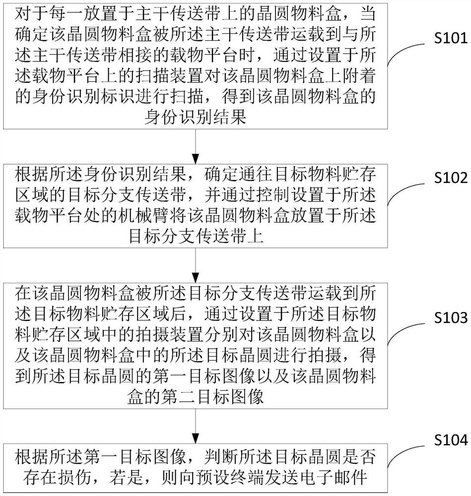
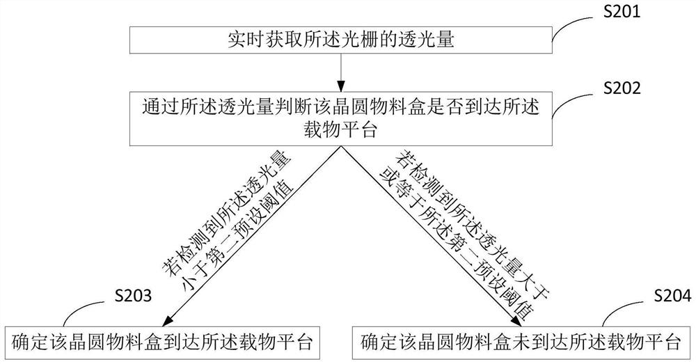
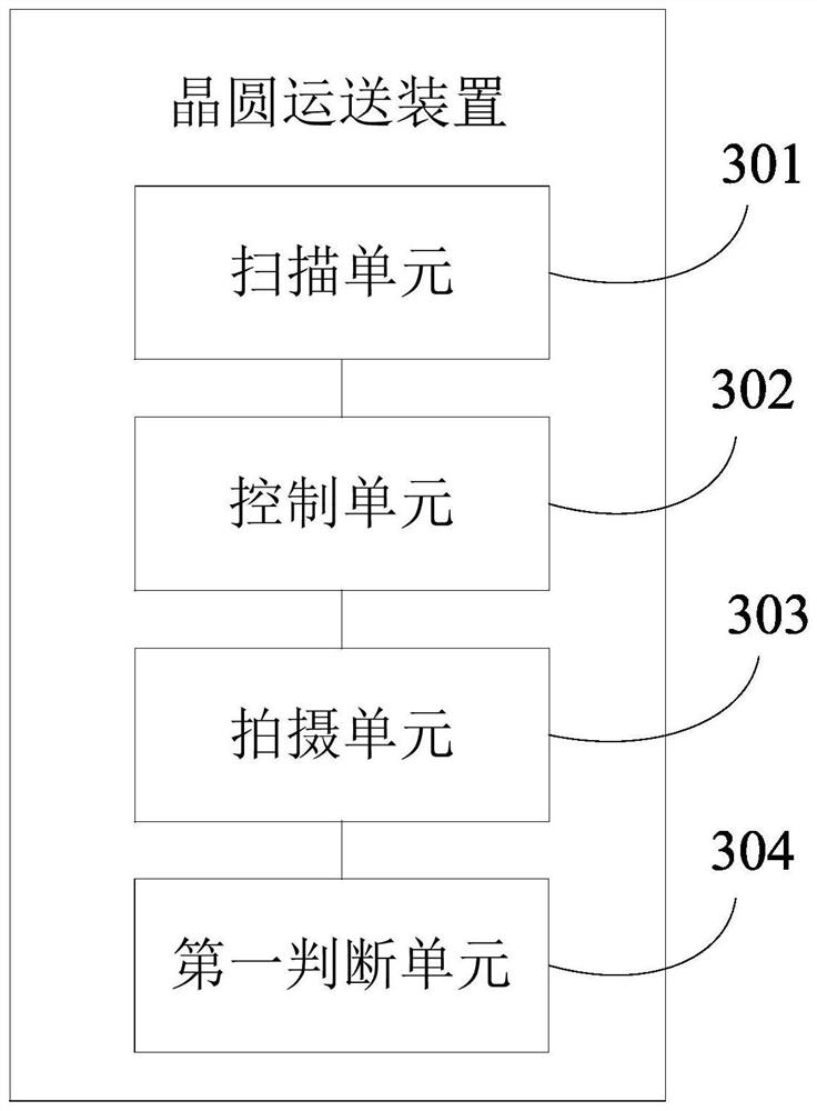
[0049] In order to make the purpose, technical solutions and advantages of the embodiments of the present application clearer, the technical solutions in the embodiments of the present application will be clearly and completely described below in conjunction with the drawings in the embodiments of the present application. It should be understood that the appended The figures are only for the purpose of illustration and description, and are not used to limit the protection scope of the present application. Additionally, it should be understood that the schematic drawings are not drawn to scale. The flowcharts used in this application illustrate operations implemented in accordance with some embodiments of the application. It should be understood that the operations of the flowcharts may be performed out of order, and steps that have no logical context may be performed in reverse order or concurrently. In addition, those skilled in the art may add one or more other operations t...


PUM


Abstract

The invention provides a wafer conveying method and device, electronic equipment and a storage medium, and the method comprises the steps: for each wafer material box, when the wafer material box is conveyed to a carrying platform by a main conveying belt, scanning an identification mark on the wafer material box, and obtaining an identification result; according to the recognition result, a target branch conveying belt leading to the target material storage area is determined, and the wafer material box is placed on the target branch conveying belt through a mechanical arm; after the wafer material box is carried to a target material storage area, shooting the wafer material box and a target wafer to obtain a target image; and according to the target image, judging whether the target wafer is damaged, and if yes, sending an E-mail to a preset terminal. According to the invention, automatic conveying of the wafer material box can be realized, and when the wafer in the wafer material box is damaged in the conveying process, a worker is notified by a mail, so that subsequent use of the damaged wafer for processing operation and the like is avoided.

Description

technical field [0001] The present application relates to the field of semiconductors, in particular, to a method, device, electronic equipment and storage medium for wafer delivery. Background technique [0002] Wafer refers to the silicon wafer used in the production of silicon semiconductor integrated circuits. Because of its circular shape, it is called a wafer. With the development of the times and the continuous advancement of integrated circuit technology, more and more wafers are being produced. [0003] After the wafer is fabricated, the wafer needs to be stored in a material storage area specially used for storing the wafer (different material storage areas are used for storing different types of wafers). However, in the prior art, it is necessary to manually transport the wafer material box loaded with wafers, thus greatly increasing labor costs. Contents of the invention [0004] In view of this, the purpose of this application is to provide a wafer transport...

Claims


Application Information

Patent Timeline
Patent Type & Authority Applications(China)
IPC IPC(8): B65G15/22B65G47/74G06Q10/10H01L21/67
CPCB65G15/22B65G47/74G06Q10/107H01L21/67276Y02P90/30
Inventor 高军
Owner 赛美特科技有限公司
Why Eureka
Try Eureka