FPGA (Field Programmable Gate Array) chip layout method, device and equipment
A chip layout and chip technology, applied in computer-aided design, instrumentation, computing, etc., can solve problems such as circuit delay violations, reduce layout flexibility, etc., and achieve the effect of improving quality
- Summary
- Abstract
- Description
- Claims
- Application Information
AI Technical Summary
Problems solved by technology
Method used
Image
Examples
Embodiment Construction
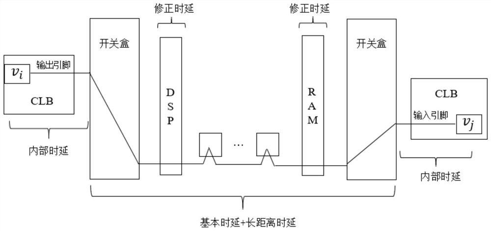
[0099] The FPGA chip adopts a regular array structure, and the points in the array can be modules, including Configurable Logic Block (CLB), Input Output Block (IOB), Digital Signal Processor (Digital Signal Processor, DSP), random access memory (Random Access Memory, RAM), etc.; modules (such as CLB, DSP, RAM) include circuit elements such as look-up tables (Look Up Table, LUT), flip-flops (Flip-Flop, FF).
[0100] Modules such as CLB include a Switch Box and many segments. The Switch Box describes the topological connection that converts any segment to the remaining segments through an optional programmable interconnection point (Programmable Interconnection Point, PIP). , multiple segments connected through Switch Box and PIP can form a wire network (net) from one circuit element to another circuit element.
[0101] A segment may pass through multiple modules, and the length type of the segment can be defined according to the number of modules passed through. For example, t...
PUM
 Abstract
Description
Claims
Application Information


