High-electron-mobility transistor epitaxial wafer capable of improving preparation efficiency and preparation method

A technology with high electron mobility and preparation efficiency, which is applied in the field of high electron mobility transistor epitaxial wafers and its preparation, can solve problems such as the unsatisfactory growth efficiency of HEMT epitaxial wafers, and achieve the promotion of nucleation and growth efficiency, good connection effect, and improved The effect of preparation efficiency

Pending Publication Date: 2022-04-29
HC SEMITEK ZHEJIANG CO LTD
View PDF0 Cites 0 Cited by
  • Summary
  • Abstract
  • Description
  • Claims
  • Application Information

AI Technical Summary

Problems solved by technology

[0003] HEMT epitaxial wafers are often grown using a silicon substrate as a substrate, but there is a large lattice mismatch between the silicon substrate and the gallium nitride material, even if an AlN layer and an AlGaN layer are added between the silicon substrate and the gallium nitride material buffer layer to relieve lattice mismatch, the quality of gallium nitride materials such as GaN high resistance layer grown on the AlGaN buffer layer; if grow gallium nitride material at a lower growth rate to improve the The quality of gallium nitride materials such as high-resistance layers, the growth efficiency of HEMT epitaxial wafers is not ideal

Method used


Image

  • High-electron-mobility transistor epitaxial wafer capable of improving preparation efficiency and preparation method
  • High-electron-mobility transistor epitaxial wafer capable of improving preparation efficiency and preparation method
  • High-electron-mobility transistor epitaxial wafer capable of improving preparation efficiency and preparation method

Examples


Embodiment Construction

[0027] In order to make the purpose, technical solution and advantages of the present disclosure clearer, the implementation manners of the present disclosure will be further described in detail below in conjunction with the accompanying drawings.

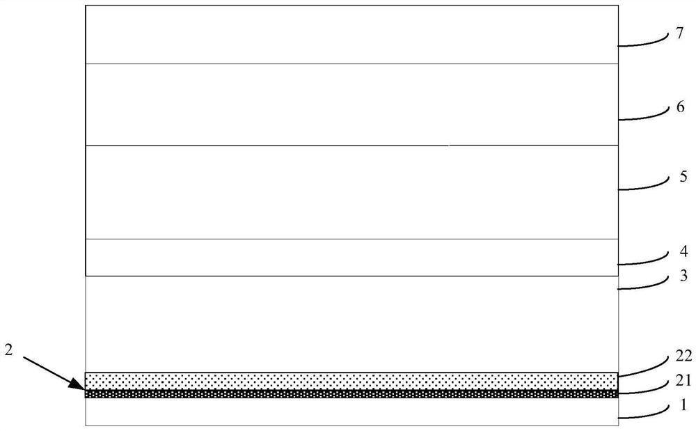
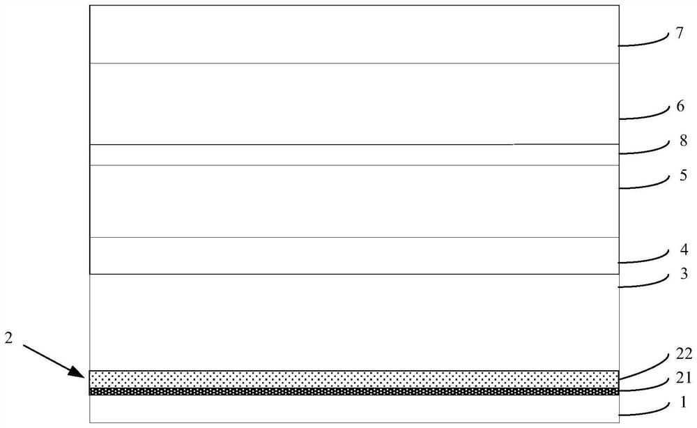
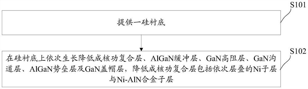
[0028] figure 1 It is a schematic structural diagram of a high electron mobility transistor epitaxial wafer that improves the preparation efficiency provided by the embodiment of the present disclosure. Refer to figure 1 It can be seen that the embodiment of the present disclosure provides a high electron mobility transistor epitaxial wafer, and the high electron mobility transistor epitaxial wafer with improved production efficiency includes a silicon substrate 1 and a composite layer stacked on the silicon substrate 1 to reduce the nucleation work. 2. AlGaN buffer layer 3, GaN high-resistance layer 4, GaN channel layer 5, AlGaN barrier layer 6 and GaN capping layer 7, and the composite layer 2 for reducing nucleation work include...


PUM

PropertyMeasurementUnit
thicknessaaaaaaaaaa
thicknessaaaaaaaaaa
temperatureaaaaaaaaaa

Abstract

The invention provides a high-electron-mobility transistor epitaxial wafer capable of improving preparation efficiency and a preparation method, and belongs to the technical field of semiconductor devices. The Ni sub-layer and the Ni-AlN alloy sub-layer are stacked on the silicon substrate, and the Ni sub-layer is high in density, so that the quality of an epitaxial material grown on the Ni sub-layer is improved. The connection effect between the Ni-AlN alloy sub-layer on the Ni sub-layer and the Ni sub-layer is good, gallium nitride materials grow on the Ni-AlN alloy sub-layer in a heterogeneous nucleation mode and then grow on the basis of crystal nucleuses, the nucleation work of the heterogeneous nucleation is low, the AlGaN buffer layer doped with Al and the Ni-AlN alloy sub-layer are made of homogeneous materials, rapid growth can be achieved, and the performance of the AlGaN buffer layer is improved. Meanwhile, heterogeneous nucleation also exists in the AlGaN buffer layer, rapid growth of the AlGaN buffer layer can be promoted, the quality of the AlGaN buffer layer can be guaranteed, and the preparation efficiency of the finally obtained high-electron-mobility transistor is effectively improved.

Description

technical field [0001] The present disclosure relates to the technical field of semiconductor devices, in particular to a high electron mobility transistor epitaxial wafer and a preparation method for improving preparation efficiency. Background technique [0002] HEMT (High Electron Mobility Transistor, High Electron Mobility Transistor) is a heterojunction field effect transistor, which is widely used in various electrical appliances. The HEMT epitaxial wafer is the basis for preparing HEMT devices. The HEMT epitaxial wafer includes a substrate and an AlN layer, an AlGaN buffer layer, a GaN high resistance layer, a GaN channel layer, an AlGaN barrier layer and a GaN capping layer stacked on the substrate in sequence. [0003] HEMT epitaxial wafers are often grown using a silicon substrate as a substrate, but there is a large lattice mismatch between the silicon substrate and the gallium nitride material, even if an AlN layer and an AlGaN layer are added between the silicon...

Claims


Application Information

Patent Timeline
Patent Type & Authority Applications(China)
IPC IPC(8): H01L29/778H01L29/10H01L21/02H01L21/335
CPCH01L29/7786H01L29/1075H01L21/02381H01L21/02458H01L21/02491H01L21/0254H01L29/66462
Inventor 蒋媛媛刘旺平
Owner HC SEMITEK ZHEJIANG CO LTD
Why Eureka
Try Eureka