

Nanofluidic chip processing method based on carbon nanotube channel
A carbon nanotube and processing method technology, applied in the field of nanofluidic chip processing, can solve the problems of destroying the integrity of the carbon nanotube wall, poor mechanical stability of the lipid layer, inconvenient chip integration, etc., to achieve integrity , good integrity and high production efficiency
- Summary
- Abstract
- Description
- Claims
- Application Information
AI Technical Summary
Problems solved by technology
Method used
Image

Examples
Embodiment 1
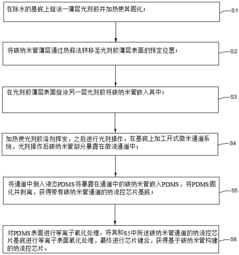
[0048] The concrete method of this embodiment is as follows:
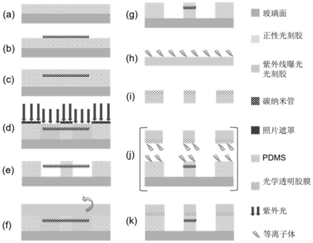
[0049] Such as figure 2 (a) A thin layer of photoresist is spin-coated on a water-removing substrate and cured by heating. The substrate used is a silicon wafer with a thickness of 1mm. The silicon wafer is heated to 150°C under normal pressure and kept for 30 minutes to remove water, and then spin-coated on the silicon wafer immediately after the silicon wafer is cooled. The spin-coated photoresist is SU8-3005, spin-coated with a thickness of 5 μm, heated at 95°C for 2 minutes after spin-coating to completely evaporate the solvent;
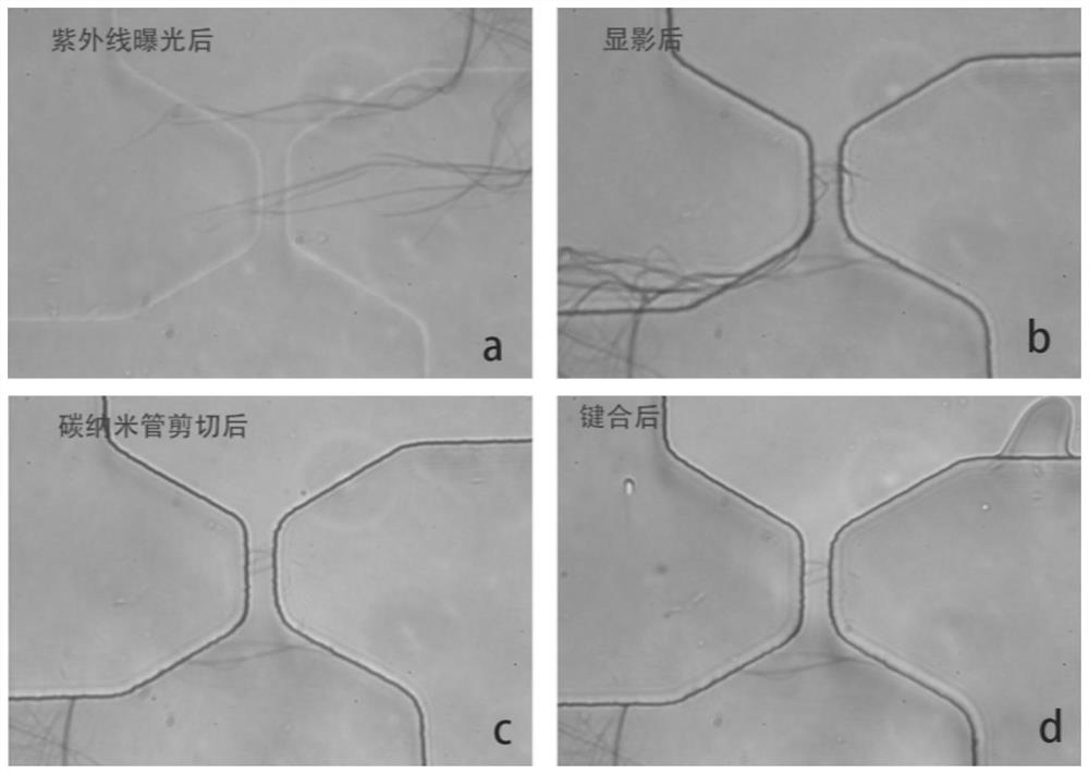
[0050] The carbon nanotube thin layer is transferred to a predetermined position on the surface of the photoresist thin layer by a pyrolysis method. The specific steps and parameters are as follows: Figure 4 (a), using an adhesive tape to separate a bundle of carbon nanotubes from the bundles of carbon nanotubes vertically grown on the silicon wafer, the inner diameter of the car...
PUM
| Property | Measurement | Unit |
|---|---|---|
| Thickness | aaaaa | aaaaa |
Abstract
Description
Claims
Application Information