Structure with conductive pattern and method for manufacturing same

A manufacturing method and structure technology, which can be used in cable/conductor manufacturing, printed circuit manufacturing, radiation element structure, etc., can solve the problems of requiring photoresist materials, complexity, and many processes, and achieve a simple interlayer The effect of tightness

Pending Publication Date: 2022-05-06
ASAHI KASEI KK
View PDF1 Cites 0 Cited by
  • Summary
  • Abstract
  • Description
  • Claims
  • Application Information

AI Technical Summary

Problems solved by technology

However, the existing methods have the disadvantages of many steps, complicated procedures, and the need for photoresist materials.

Method used


Image

  • Structure with conductive pattern and method for manufacturing same
  • Structure with conductive pattern and method for manufacturing same
  • Structure with conductive pattern and method for manufacturing same

Examples


Embodiment 1

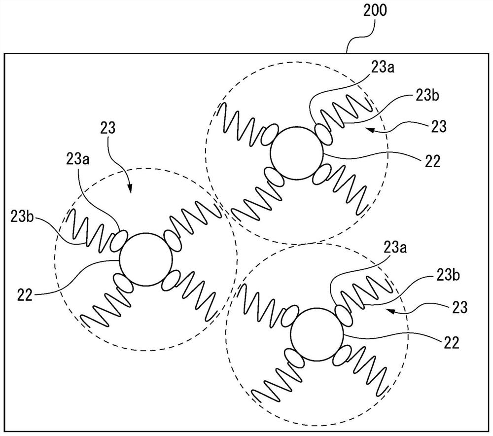
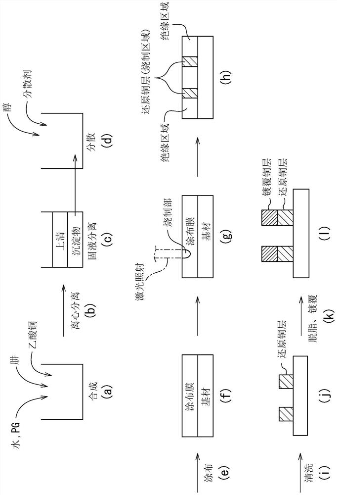
[0234] Dissolve 806 g of copper acetate (II) monohydrate (manufactured by Kanto Chemical Co., Ltd.) in a mixed solvent of 7560 g of distilled water (manufactured by Kyoei Pharmaceutical Co., Ltd.) and 3494 g of 1,2-propanediol (manufactured by Kanto Chemical Co., Ltd.). The thermostat keeps the liquid temperature at -5°C. Add 235 g of hydrazine monohydrate (manufactured by Tokyo Chemical Industry Co., Ltd.) over 20 minutes, stir in a nitrogen atmosphere for 30 minutes, then set the liquid temperature to 25° C. with an external thermostat, and stir in a nitrogen atmosphere for 90 minutes. After stirring, the supernatant and the precipitate were separated by centrifugation. 13.7 g of Disper BYK-145 (manufactured by BYK Chemicals, a phosphoric acid group-containing organic compound) (dispersant content 4 g) and 907 g of ethanol (manufactured by Kanto Chemical Co., Ltd.) were added to 390 g of the obtained precipitate, and the mixture was used in a nitrogen atmosphere. Dispersion...

Embodiment 2

[0245] The dispersion obtained in the same manner as in Example 1 was applied to a polyimide film (manufactured by Toray-DuPont, KAPTON500H, thickness 125 μm) by spin coating, and kept in an oven at 90° C. for 2 hours. The solvent in the film evaporated, and Sample 2 was obtained. The coating film thickness of the obtained sample 2 was 1000 nm.

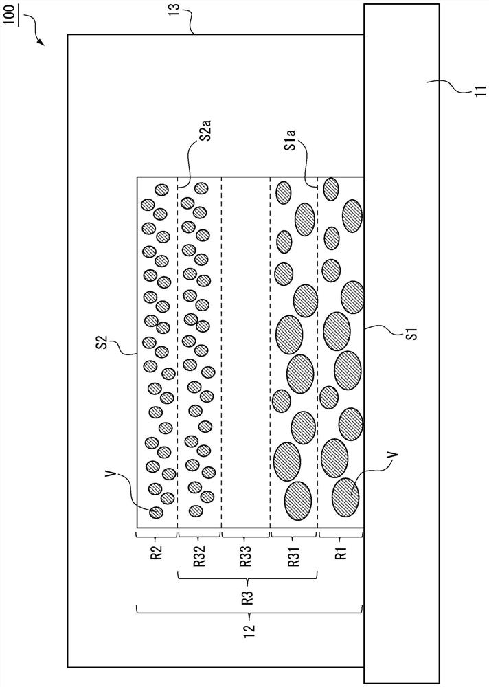
[0246] Using a Galvano scanner, irradiate laser light (pulse wave oscillation, 532 nm) to the coating film of sample 2 while moving the focus position at a maximum speed of 4500 mm / min, thereby obtaining a desired size of 0.5 mm × 5 mm. Conductive pattern area (copper-containing film). The coating film remained in the area not irradiated with laser light.

[0247] The cross-section of copper in the conductive pattern region was observed by SEM. As a result, the thickness was 0.5 μm, and the porosity was 40% by volume in the region on the first main surface side. In addition, the resistance value of the conductive pattern region was...

Embodiment 3

[0252] The dispersion obtained in the same manner as in Example 1 was applied to a polyimide film (manufactured by Toray-DuPont, KAPTON500H, thickness 125 μm) by spin coating, and kept in an oven at 90° C. for 2 hours. The solvent in the film evaporated, and Sample 3 was obtained. The coating film thickness of the obtained sample 3 was 1000 nm.

[0253] Using a Galvano scanner, irradiate laser light (pulse wave oscillation, 532 nm) to the coating film of sample 3 while moving the focus position at a maximum speed of 1200 mm / min, thereby obtaining a desired size of 0.5 mm × 5 mm. Conductive pattern area (copper-containing film). The coating film remained in the area not irradiated with laser light.

[0254] The cross-section of copper in the conductive pattern region was observed by SEM, and the thickness was 0.5 μm, and the porosity was 11.7% by volume in the region on the first main surface side. In addition, the resistance value of the conductive pattern region was 30 μΩc...


PUM

PropertyMeasurementUnit
thicknessaaaaaaaaaa
thicknessaaaaaaaaaa
thicknessaaaaaaaaaa

Abstract

Provided are: a structure with a conductive pattern, which can be obtained by a simple manufacturing process and has good interlayer adhesion; and a method for manufacturing the structure. One embodiment of the present invention provides a structure with a conductive pattern, which is provided with a base material and a conductive layer that is arranged on the surface of the base material and contains copper, and wherein: when the main surface of the conductive layer on the side facing the base material is a first main surface and the main surface on the opposite side from the first main surface is a second main surface, the first main surface and the second main surface are opposite to each other; the conductive layer has a porosity of 0.01% by volume or more and 50% by volume or less in a first main surface-side region extending from the first main surface to a depth of 100 nm in the thickness direction of the conductive layer, and has a porosity of 10% by volume or less in a second main surface-side region extending from the second main surface to a depth of 100 nm in the thickness direction of the conductive layer.

Description

technical field [0001] The present invention relates to a structure with a conductive pattern and a manufacturing method thereof. Background technique [0002] The circuit board has a structure in which conductive wiring is provided on the board. The manufacturing method of a circuit board is generally as follows. First, a photoresist is applied to a substrate bonded with a metal foil. Next, the photoresist is exposed and developed to obtain a desired circuit pattern in the shape of a bottom plate. Afterwards, the portion of the metal foil not covered by the photoresist is removed by chemical etching to form a pattern. Thereby, a high-performance circuit board can be manufactured. However, the existing methods have disadvantages such as a large number of steps, complicated procedures, and the need for photoresist materials. [0003] In contrast, the method of directly printing a desired wiring pattern on a substrate using a dispersion in which fine particles selected fr...

Claims


Application Information

Patent Timeline
Patent Type & Authority Applications(China)
IPC IPC(8): H05K1/09H05K3/18H05K3/22H01B5/14H01B13/00
CPCH05K1/092H05K3/18H05K3/227H01B5/14H01B13/00C23C18/40H01Q1/526C23C18/405C23C18/1651C23C18/143C23C18/1648C23C18/1608C23C18/08C23C18/1879C23C18/206C09D11/037C09D11/52H05K3/105H05K2203/107H05K2203/121H05K3/244H05K2201/0209C25D3/38H05K3/384C23C18/14C23C18/18H01Q1/38C23C18/165C23C18/1875H05K1/0237H05K1/09H05K3/10
Inventor 小园智子汤本徹
Owner ASAHI KASEI KK
Why Eureka
Try Eureka