PCB warping detection device, method and system

A PCB board and detection device technology, applied in the field of PCB board warpage detection devices, can solve the problems of increasing processing steps, inaccurate detection, board surface pollution, etc., and achieve flexible and accurate detection, avoid detection missed detection, and high detection accuracy. Effect

Pending Publication Date: 2022-05-13
上海威固信息技术股份有限公司
View PDF9 Cites 0 Cited by
  • Summary
  • Abstract
  • Description
  • Claims
  • Application Information

AI Technical Summary

Problems solved by technology

If the plug gauge can be moved into the PCB board from this end corner, it means that the bending degree of the PCB board exceeds the tolerance range and is not suitable for subsequent assembly operations. If the plug gauge cannot be moved into the end corner, it means that the bending degree of the PCB board is within acceptable tolerances within the range
However, this method of detecting the bending degree of the PCB board needs to manually pick up the plug gauge, which is time-consuming and labor-intensive, and it is easy to cause inaccurate detection. The operation process is likely to cause board surface pollution, finger prints and other quality abnormalities, and increase the processing steps. In addition, the existing detection methods cannot realize arbitrary switching detection of PCB boards of different thicknesses
[0006] However, for high-speed, high-frequency, and high-density PCB boards, the tolerance for warpage is lower, and the angle of the traditional feeler gauge detection method cannot meet the demand.

Method used


Image

  • PCB warping detection device, method and system
  • PCB warping detection device, method and system
  • PCB warping detection device, method and system

Examples


Embodiment 1

[0037] In order to solve the relevant technical problems raised in the background art, this embodiment proposes a PCB warpage detection device and method, especially for high-density PCB boards and special-shaped asymmetric PCB boards, to achieve accurate and efficient detection of their warpage.

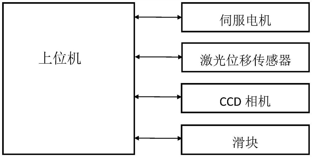
[0038] Such as figure 1 As shown, the PCB warpage detection device includes a detection table arranged under the detection device. The detection table is used to carry and position the PCB board to be tested. When testing, the PCB board to be detected is positioned on the detection table. The mature positioning methods in the prior art, such as positioning clamps and positioning screws, are used to position the PCB to be tested, which will not be repeated here.

[0039] In this embodiment, a slider and a servo motor that can slide in any direction along the XY plane are arranged directly above the detection device, and the servo motor can drive the slider to slide precisely in the X...

Embodiment 2

[0054] This embodiment is further improved on the basis of Embodiment 1, and the common parts of the technical solutions will not be repeated here.

[0055] This embodiment also provides a PCB warpage detection method, which is supposed to realize the detection of PCB warpage according to the PCB warpage detection in Embodiment 1. Such as Figure 4 As shown, the method specifically includes the following steps:

[0056] Step S1. Generate a detection path for local detection. Input the original design CAD layout of the PCB board to the host computer, and generate the detection path according to the CAD layout;

[0057] In this embodiment, the detection path is determined by the edge of the PCB board and the position of key components. This step can realize the detection of key parts of special-shaped asymmetric PCB or high-speed PCB, and improve the efficiency of detection.

[0058] Step S2, performing local warpage detection. The host computer controls the servo motor to d...

Embodiment 3

[0069] This embodiment is further improved on the basis of embodiment 1 or embodiment 2, and the common parts of the technical solutions will not be repeated here.

[0070] This embodiment provides a PCB warpage detection system. The detection system adopts the detection device in Embodiment 1 and the detection method provided in Embodiment 2 to realize the detection of PCB warpage. The system includes a feeding module, a detection module and unloading module.

[0071] The loading module is used to place the PCB board to be tested on the detection table. The detection module adopts the detection method provided in Embodiment 2 to detect the warpage of the PCB board to be tested, and the unloading module unloads the detected PCB board. In this embodiment, the unqualified PCB boards are eliminated, and the qualified PCB boards are sent to the next process.


PUM


Abstract

The invention provides a PCB warpage detection device, method and system, and the device is provided with a detection platform which carries and positions a to-be-detected PCB. The sliding block is arranged above the detection table and can accurately slide in an XY plane; the laser displacement sensor and the CCD camera are arranged on the sliding block, the optical axis of the laser displacement sensor is vertically downward, and the CCD camera collects light spot images of the laser displacement sensor; and the upper computer is used for planning a detection path according to the CAD layout of the PCB to be detected and controlling the detection device at the same time. According to the invention, the warping of the PCB is detected in a manner of carrying out local scanning detection on the part easy to warp and then carrying out overall offset detection, so that high-precision detection and high-efficiency detection on the warping of the PCB are realized.

Description

technical field [0001] The invention relates to the field of PCB circuit board detection, in particular to a PCB board warpage detection device, method and system. Background technique [0002] With the rapid development of the electronics industry and the widespread use of SMT automation plug-in equipment and placement equipment, the quality requirements for printed boards are also getting higher and higher. While electronic products are developing in the direction of high speed, high frequency, high density and multi-function, the warping problem of printed circuit boards is becoming increasingly prominent during electronic assembly. If the flatness of the printed circuit board does not meet the requirements, it will cause material throwing, false soldering, or even failure to solder. Nowadays, with the emergence of HDI boards and IC substrates, and the application of a large number of SMT components and IC chips, especially semiconductor chips such as processors, control...

Claims


Application Information

Patent Timeline
Patent Type & Authority Applications(China)
IPC IPC(8): G01B11/16
CPCG01B11/167
Inventor 吴佳
Owner 上海威固信息技术股份有限公司
Why Eureka
Try Eureka