Integrated packaging structure based on TSV silicon switching substrate stacking and manufacturing method

A technology of integrated packaging and manufacturing methods, applied in the field of integrated packaging structure and manufacturing based on TSV silicon transfer substrate stacking, can solve the problems of small size of TSV silicon transfer substrate, low integration density, limited number of integrated chips, etc., and achieve improvement Effects of signal integrity, high I/O integration density, and shortened interconnection distance

Pending Publication Date: 2022-05-13
珠海天成先进半导体科技有限公司
View PDF1 Cites 0 Cited by
  • Summary
  • Abstract
  • Description
  • Claims
  • Application Information

AI Technical Summary

Problems solved by technology

[0004] In order to overcome the shortcomings of the above-mentioned prior art, the purpose of the present invention is to provide a multi-chip integrated package structure and manufacturing method based on TSV silicon transfer substrate stacking, so as to solve the problem of the small size of the TSV silicon transfer substrate and the limited number of integrated chips in the prior art. , low integration density in the Z-axis direction of the substrate, etc.

Method used


Image

  • Integrated packaging structure based on TSV silicon switching substrate stacking and manufacturing method
  • Integrated packaging structure based on TSV silicon switching substrate stacking and manufacturing method
  • Integrated packaging structure based on TSV silicon switching substrate stacking and manufacturing method

Examples


Embodiment Construction

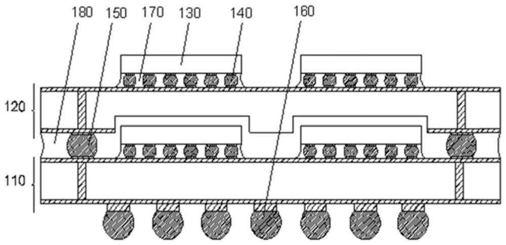
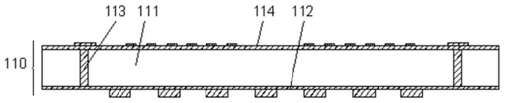
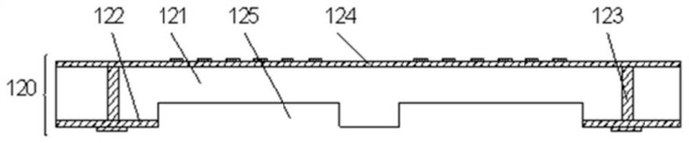
[0042] In order to enable those skilled in the art to better understand the solutions of the present invention, the following will clearly and completely describe the technical solutions in the embodiments of the present invention in conjunction with the drawings in the embodiments of the present invention. Obviously, the described embodiments are only It is an embodiment of a part of the present invention, but not all embodiments. Based on the embodiments of the present invention, all other embodiments obtained by persons of ordinary skill in the art without making creative efforts shall fall within the protection scope of the present invention.

[0043] It should be noted that the terms "first", "second" and the like in the description and claims of the present invention and the above drawings are used to distinguish similar objects, and are not necessarily used to describe a specific sequence or sequence. It is to be understood that the data so used may be interchanged unde...


PUM


Abstract

The invention discloses an integrated packaging structure based on TSV silicon switching substrate stacking and a manufacturing method, and belongs to the technical field of integrated circuit packaging. Comprising a TSV silicon switching substrate, a TSV silicon-based cavity switching substrate, a switching substrate interconnection structure, a TSV silicon switching substrate external solder ball, a first bottom filling structure, a second bottom filling structure, a microelectronic chip and a chip and switching plate interconnection structure. The TSV silicon-based cavity switching substrate is connected with the TSV silicon switching substrate through the interconnection structure between the switching substrates, the microelectronic chip is connected with the TSV silicon switching substrate through the chip and switching plate interconnection structure, the first bottom filling structure is located between the TSV microelectronic chip and the TSV silicon switching substrate, and the second bottom filling structure is located between the two substrates. According to the multi-chip integrated packaging structure, the system packaging size is reduced, the interconnection density is improved, the interconnection distance is shortened, the transmission delay is reduced, the bandwidth is improved, and the power supply efficiency is improved.

Description

technical field [0001] The invention belongs to the technical field of integrated circuit packaging, and in particular relates to an integrated packaging structure and a manufacturing method based on stacking of TSV silicon transfer substrates. Background technique [0002] PoP, Packaging on Packaging, that is, stacked assembly, also known as stacked packaging. PoP adopts two or more BGAs, a packaging method in which ball grid array packages are stacked. Generally, the PoP stacked packaging structure adopts the BGA solder ball structure, and the digital or mixed-signal logic device is integrated at the bottom of the PoP package to meet the characteristics of multiple pins of the logic device. PoP packaging can realize multi-layer stacking, save the substrate area, and realize multi-chip integration in the vertical direction. [0003] The domestic patent "package-in-package device and its manufacturing method" patent number CN201310549390.3 discloses a package-in-package de...

Claims


Application Information

Patent Timeline
Patent Type & Authority Applications(China)
IPC IPC(8): H01L23/48H01L25/065H01L25/18H01L21/50H01L21/60H01L21/768
CPCH01L23/481H01L25/0652H01L25/18H01L21/50H01L21/76898H01L2021/60007H01L2021/60022H01L2224/73204H01L2224/16225H01L2224/32225H01L2224/92125H01L2924/00
Inventor 张辽辽吴道伟唐磊刘建军姚华
Owner 珠海天成先进半导体科技有限公司
Why Eureka
Try Eureka