Wafer processing device and method

A processing device and processing method technology, applied in the manufacturing of electrical components, circuits, semiconductor/solid-state devices, etc., can solve the problems of inability to remove flue gas, loss of wafer yield, etc., to prevent the equipment from becoming larger and expand the manufacturing space , The effect of improving product yield

Pending Publication Date: 2022-05-20
INST OF MICROELECTRONICS CHINESE ACAD OF SCI +1
View PDF0 Cites 0 Cited by
  • Summary
  • Abstract
  • Description
  • Claims
  • Application Information

AI Technical Summary

Problems solved by technology

[0005] In view of the above analysis, the present invention aims to provide a wafer processing device and method to solve the problem that in the prior art, cleaning is performed after all wafer processes have been performed, resulting in the inability to completely remove the flue gas generated during the semiconductor manufacturing process. removal, wafer yield loss issues

Method used


Image

  • Wafer processing device and method
  • Wafer processing device and method
  • Wafer processing device and method

Examples


Embodiment 1

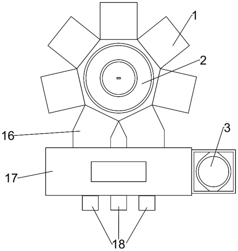
[0038] A specific embodiment of the present invention discloses a wafer processing device, such as figure 1 shown. The wafer processing apparatus includes a process chamber 1 , a transfer chamber 2 , a cleaning system 3 , a pre-evacuation chamber 16 , an atmospheric transfer chamber 17 and a rack 18 . Process chambers may include etch chambers or deposition chambers or injection chambers. The transfer chamber 2 is provided with a transfer robot, and the transfer of the wafer between the process chamber 1 and the transfer chamber 2 and between the transfer chamber 2 and the cleaning system 3 is completed by the transfer robot.

[0039] In a possible implementation manner, the cleaning system 3 is set in the wafer processing device, so that the wafers processed by the etching chamber, the deposition chamber or the injection chamber can directly enter the cleaning system 3 for cleaning.

[0040] In order to prevent the volume of the cleaning system 3 from becoming larger after ...

Embodiment 2

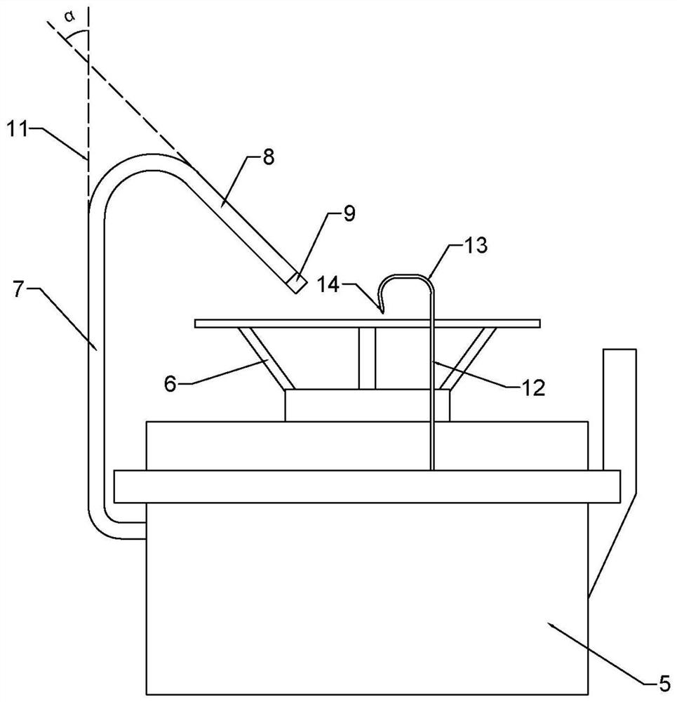
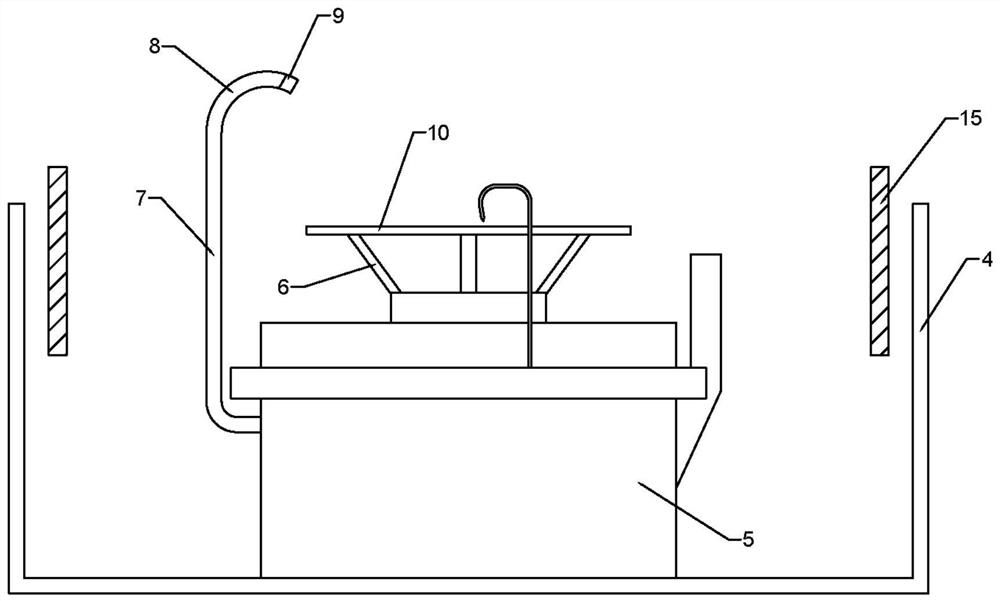
[0055] Another embodiment of the present invention discloses a wafer processing method, which includes the transfer robot in the transfer chamber picking up the wafer and placing it in the process chamber, and after the wafer is processed, the transfer robot picks up the wafer again and places it in the cleaning The system is cleaned and dried.

[0056] Because the wafer manufacturing process usually requires multiple processes, there are also multiple processes that generate fumes, such as etching processes, deposition processes, and implant processes. In the wafer processing method of the present invention, after each fume-generating process is completed, the wafer is immediately sent to the cleaning system for cleaning and drying without any delay, so that the fume will not flow on the wafer. The surface is solidified, so that the removal of smoke is more thorough, and effectively prevents yield loss.

[0057] The etching process is taken as an example below to describe th...


PUM


Abstract

The invention relates to a wafer processing device and method, belongs to the technical field of semiconductor manufacturing, and solves the problems that in the prior art, cleaning is carried out after all wafer processes are completed, smoke generated in the semiconductor manufacturing process cannot be completely removed, and the wafer yield is lost. The wafer processing device comprises a process chamber, a transfer chamber and a cleaning system. The cleaning system is arranged in the wafer processing device, so that the wafer passing through the process chamber can directly enter the cleaning system to be cleaned. A transfer mechanical arm is arranged in the transfer chamber, and the transfer mechanical arm completes the transfer of the wafer between the process chamber and the transfer chamber and between the transfer chamber and the cleaning system. The wafer processing method comprises the steps that after each process capable of generating smoke is carried out, the wafer is conveyed into the cleaning system to be cleaned and dried. According to the invention, the flue gas is effectively removed, and the yield loss caused by the flue gas is improved.

Description

technical field [0001] The invention relates to the technical field of semiconductor manufacturing, in particular to a wafer processing device and method. Background technique [0002] During the semiconductor manufacturing process, the fume generated by the etching, deposition, and implantation (Implantation) processes will pollute the wafer. The fume left on the wafer solidifies over time and becomes a defect source (Defect Source), resulting in a decline in product yield. [0003] In order to remove such fumes, various improvements have been made in the prior art. A typical way to deal with it is to set N 2 Stocker, Ammonia Filter, Buffer Station and Side Storage. [0004] However, the existing cleaning equipment and the process chamber are usually set independently, so that the cleaning can only be performed after all the wafer processes have been performed, thus causing the fume left on the wafer to solidify over time, resulting in inability to Complete removal of s...

Claims


Application Information

Patent Timeline
IPC IPC(8): H01L21/67H01L21/02
CPCH01L21/67155H01L21/67207H01L21/67051H01L21/67034H01L21/02057H01L21/02082H01L21/02087
Inventor 姜东勋周娜李俊杰王佳李琳
Owner INST OF MICROELECTRONICS CHINESE ACAD OF SCI
Why Eureka
Try Eureka