Unlock instant, AI-driven research and patent intelligence for your innovation.

Low-noise weak signal detection interface circuit capable of realizing independent regulation and control of gain and bandwidth

A weak signal detection and interface circuit technology, applied in the direction of logic circuit interface device, logic circuit connection/interface layout, reliability improvement and modification, etc., can solve difficult problems such as bandwidth, gain and noise, difficult detection, noise aliasing, etc. , to achieve high use and promotion value, improve signal-to-noise ratio, and low equivalent input current noise

Pending Publication Date: 2022-05-27
NANJING UNIV OF SCI & TECH
View PDF0 Cites 0 Cited by
  • Summary
  • Abstract
  • Description
  • Claims
  • Application Information

AI Technical Summary

Problems solved by technology

[0004] For the weak detection current signal, its value is usually at the nA level, which is very susceptible to noise interference or even submerged in the noise, making detection more difficult. Therefore, the low-noise front-end amplifier interface circuit is the key to ensure the measurement accuracy of precision sensors
However, the traditional front-end amplifier is difficult to solve the constraints of gain, bandwidth, noise, power consumption and other indicators
For example, switched capacitor front-end amplifiers suffer from noise aliasing
At the same time, due to the existence of parasitic capacitance, single-stage or multi-stage traditional transimpedance amplifiers are difficult to solve the contradiction between bandwidth, gain and noise
Therefore, the design of the front-end interface circuit is a big challenge

Method used


Image

  • Low-noise weak signal detection interface circuit capable of realizing independent regulation and control of gain and bandwidth
  • Low-noise weak signal detection interface circuit capable of realizing independent regulation and control of gain and bandwidth
  • Low-noise weak signal detection interface circuit capable of realizing independent regulation and control of gain and bandwidth

Examples


Embodiment Construction

[0020] In order to make the purpose, technical solutions and advantages of the present application more clearly understood, the present application will be described in further detail below with reference to the accompanying drawings and embodiments. It should be understood that the specific embodiments described herein are only used to explain the present application, but not to limit the present application.

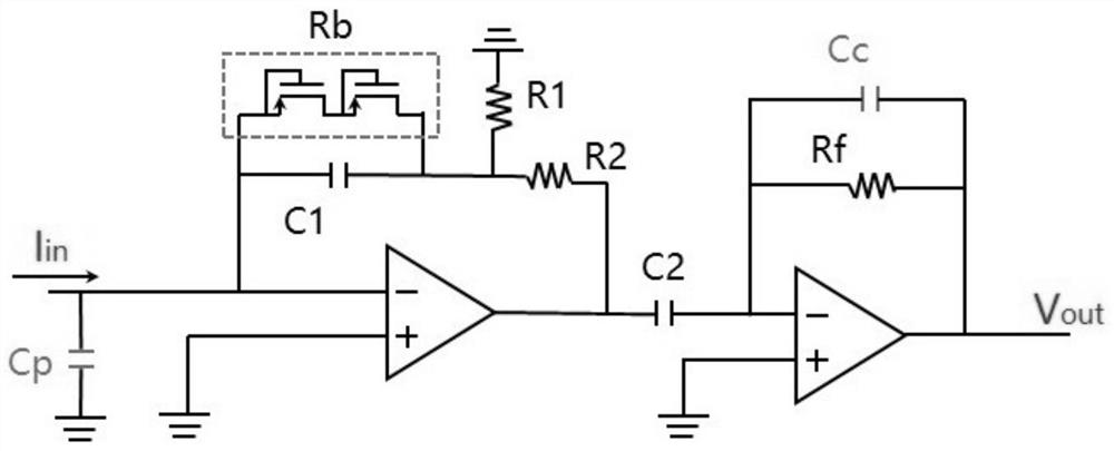
[0021] In one embodiment, combining figure 1 , provides a low-noise weak signal detection interface circuit that can realize independent control of gain and bandwidth. The circuit includes a two-stage amplification topology in series, the first stage is a T-type amplification topology, and the second stage is a transimpedance amplification topology.

[0022] The T-type amplification topology includes a first capacitor C1, a parasitic capacitor Cp, a pseudo resistor Rb, a first transconductance amplifier OTA1, and two external resistors R1 and R2; the first capacitor C1...


PUM


Abstract

The invention discloses a low-noise weak signal detection interface circuit capable of realizing independent regulation and control of gain and bandwidth. The interface circuit is used for converting a weak detection current signal of a sensor into a voltage signal. The interface circuit comprises two stages of amplification topologies: a first-stage T-type amplifier consisting of a capacitor C1, a parasitic capacitor Cp, a pseudo resistor Rb, a resistor R1, a resistor R2 and a transconductance amplifier OTA1; and the capacitor C2, the capacitor Cc, the resistor Rf and the transconductance amplifier OTA2 form a second-stage transimpedance amplifier. According to the circuit, the gain can be improved by improving the ratio of R2 / R1 and C2 / C1 without increasing Rf, the resistor Rb and the capacitor Cc can independently adjust the bandwidth, and the problem of restriction among the gain, the bandwidth and noise is greatly solved; in addition, the circuit can realize extremely low equivalent input current noise, and the signal-to-noise ratio of a detection current signal is greatly improved.

Description

technical field [0001] The invention belongs to the technical field of sensor interface circuits, in particular to the design of an I-V conversion interface circuit of a MEMS resonant sensor, in particular to a low-noise weak signal detection interface circuit capable of independent control of gain and bandwidth. Background technique [0002] Weak signals are signals that are very small in amplitude or are easily masked by ambient noise. There are many weak signals in practical engineering in various fields, and there is usually a lot of information behind these signals. Therefore, the detection of weak signals becomes particularly important. [0003] Most of the weak signal acquisition work is to use various adapted sensors to realize the acquisition work and convert it into current or voltage. For example, the photoelectric sensor converts the light signal into a weak electrical signal, and then completes the calibration of the measured light signal; the same precision fo...

Claims


Application Information

Patent Timeline
IPC IPC(8): H03K19/0175H03K19/003
CPCH03K19/017509H03K19/00346
Inventor 王皓张晶苏岩
Owner NANJING UNIV OF SCI & TECH
Features
  • R&D
  • Intellectual Property
  • Life Sciences
  • Materials
  • Tech Scout
  • Unparalleled Data Quality
  • Higher Quality Content
  • 60% Fewer Hallucinations
Learn More