

Manufacturing method and manufacturing device of electronic component
A technology of electronic components and manufacturing methods, which is applied in the field of photovoltaic device manufacturing, can solve problems such as metal plating residue and uniformity reduction of metal layers, and achieve the effects of improving uniformity, improving uniformity, and improving plating efficiency
Active Publication Date: 2022-06-03
SUZHOU MAXWELL TECH CO LTD
View PDF3 Cites 2 Cited by
- Summary
- Abstract
- Description
- Claims
- Application Information
AI Technical Summary
Problems solved by technology
Aiming at the problem that metal is easy to remain on the wire plating equipment in the prior art, which leads to a decrease in the uniformity of the metal layer, a decrease in production efficiency, and an increase in cost, the present invention provides a manufacturing method and device for electronic components. By designing a pair of wire plating rollers Semiconductor devices are plated, so that the plated roller can consume the residual metal by itself, thus effectively solving the problems of plated metal residue and reduced uniformity of the metal layer
Method used
View moreImage
Smart ImageViewing Examples

Examples
Embodiment 1
[0048] Perform the surface of the silicon wafer surface of the electroplating, select 25 points evenly, and get the uniformity value of the test results calculation, record it in Table 1.
[0049] Table 1. Different embodiments The uniformity of the surface plating of the silicon wafer surface
Embodiment 2
[0050] Perform uniform testing of the surface of the silicon wafer completed by electroplating, and record the test results in Table 1.
Embodiment 3
[0052] Perform uniform testing of the surface of the silicon wafer completed by electroplating, and record the test results in Table 1.
Login to View More PUM
| Property | Measurement | Unit |
|---|---|---|
| velocity | aaaaa | aaaaa |
| diameter | aaaaa | aaaaa |
| diameter | aaaaa | aaaaa |
Abstract
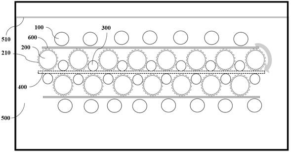
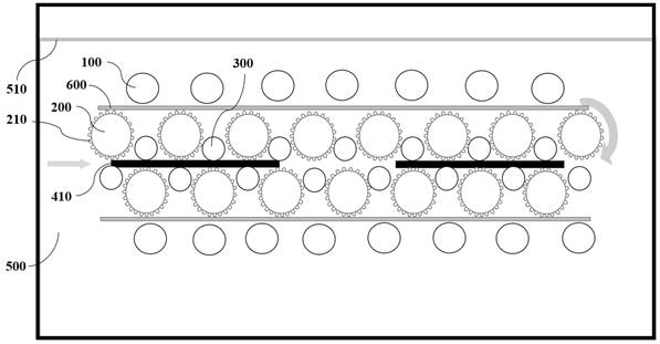
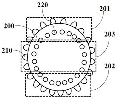
The invention discloses a manufacturing method and a manufacturing device of an electronic component, and belongs to the technical field of photovoltaic device manufacturing. The method comprises the following steps of: putting the semiconductor device into a cathode area and driving the semiconductor device to move in the cathode area, switching on a wire plating roller and driving the wire plating roller to rotate, so that a conductive part in the circumferential direction of the outer side of the wire plating roller is plated with a metal wire on the surface of the semiconductor device along the movement direction; the conductive part comprises a wire plating area and a deplating area; an anode is arranged on the outer side of the deplating area and is electrically connected with the positive pole of the power supply through a conductive part of the deplating area; a cathode area capable of placing a semiconductor device is arranged on the outer side of the wire plating area, and the semiconductor device is electrically connected with the negative electrode of the power supply through a conductive part of the wire plating area. The surface wire plating efficiency of the semiconductor device can be improved, the uniformity of a metal layer on the surface of the semiconductor device such as a silicon wafer or a battery piece is improved, and the production efficiency of an electronic element is improved.
Description
Technical field [0001] The present invention belongs to the field of photovoltaic device manufacturing technology. More specifically, it involves a manufacturing method and manufacturing device involving an electronic component. Background technique [0002] At present, the grille lines plated in the photovoltaic industry are mainly silver grid lines, copper grids, nickel grid lines, mixed grid lines, etc. The copper grid line is mainly formed by electroplating copper and light -induced. Horizontal continuous plating, etc. At present, most of the plating in the photovoltaic industry adopts the plating method. However, in the photovoltaic industry, when the plating method is used, problems such as lack of printing and surface smoothness are generally occurred, and production capacity cannot be released and the degree of equipment automation is low. In addition, in the process of hanging plating, it takes a lot of labor to install and hang the hanging and lower production efficienc...
Claims
Login to View More Application Information
Patent Timeline
 Patent Type & AuthorityApplications(China)
IPC IPC(8): C25D7/12C25D17/00C25D17/16H01L31/18
CPCC25D7/12C25D17/16C25D17/001H01L31/18Y02P70/50C25D3/38C25D5/04C25D17/005C25D21/10C25D21/11H01L21/2885
Inventor郁操董刚强
OwnerSUZHOU MAXWELL TECH CO LTD