Wafer processing method and wafer processing device

A processing method and wafer technology, applied in cleaning methods and appliances, chemical instruments and methods, cleaning methods using liquids, etc., can solve the problems of thin films affecting the stable realization of ring taking, and achieve high automation, firm fixation, and improved The effect of cutting accuracy

Active Publication Date: 2022-06-03
JIANGSU JCA ELECTRONICS TECH CO LTD
View PDF10 Cites 7 Cited by
  • Summary
  • Abstract
  • Description
  • Claims
  • Application Information

AI Technical Summary

Problems solved by technology

[0004] Moreover, in addition to the wafer position accuracy, factors such as cutting debris and film viscosity will greatly affect the stable realization of ring removal

Method used


Image

  • Wafer processing method and wafer processing device
  • Wafer processing method and wafer processing device
  • Wafer processing method and wafer processing device

Examples


Embodiment 1

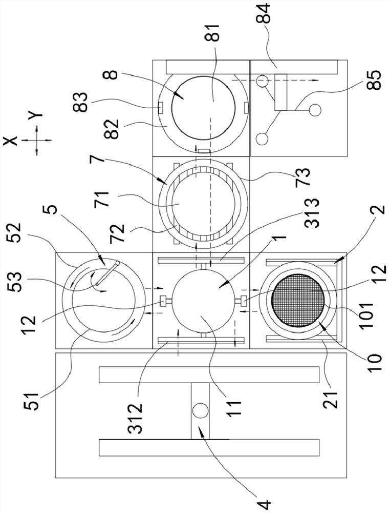
The following describes the wafer 10 processing apparatus disclosed in the present invention with reference to the accompanying drawings. figure 1 -Attached Figure 5 shown, it includes:

a worktable 1 for supporting and fixing the wafer 10, the worktable 1 can move between a first position and a second position;

The feeding mechanism 2 includes a storage box with multiple wafer placement layers and a jacking mechanism for driving the storage box to rise and fall;

The feeding mechanism 3 is used to move the wafer 10 in the feeding mechanism 2 to the worktable 1 in the first position;

The ring cutting station 4 is used to perform ring cutting processing on the wafer 10 on the worktable 1 at the second position;

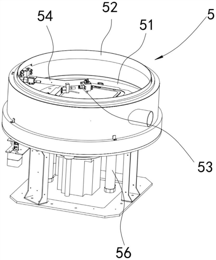
The cleaning station 5 is used for cleaning the wafer 10 located therein;

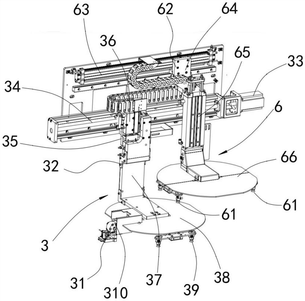
The transfer mechanism 6 is used to move the wafer 10 between the table 1 and the cleaning station 5 in the first position;

The UV debonding station 7 is used to remove the viscosity of th...

Embodiment 2

In this embodiment, on the basis of the above-mentioned Embodiment 1, the reclaiming mechanism 3 further includes a supporting mechanism. When the reclaiming robot 31 is taken out from the feeding mechanism 2, the wafer 10 is first moved to the supporting mechanism. Then move from the support mechanism to the workbench 1. Using such a feeding method can realize flexible feeding as much as possible, and reduce the risk of damage to the wafer 10 during the feeding process.

[0047] as attached figure 1 As shown, the support mechanism includes two equal-height and parallel support rails 312, which extend along the first direction X and are L-shaped, the two support rails are located on both sides of the workbench 1 and are connected to drive each An opening and closing drive mechanism (not shown in the figure) for two supporting rails to move between the third position and the fourth position, the moving directions of the two supporting rails are perpendicular to the extending di...

Embodiment 3

In S7 of the above-mentioned embodiment 1, when the support ring 101 is peeled off, the peeling blade 87 (the lower disk of the I-wheel) of the peeling robot 85 can be directly moved to its top surface and the bottom of the support ring 101 A considerable height, and peeling off after revolution.

[0054] However, in this embodiment, preferably, the S7 includes the following steps:

S71, as attached Figure 7 As shown, the peeling blade 87 of the peeling jaw 86 on which the third moving mechanism 84 drives the peeling robot 85 to move to it is located on the outer periphery of the wafer 10 on the peeling table 81 and below the wafer 10, and the peeling clamp is at this time. The upper disc 810 of the claw 86 is located above the support ring 101 .

[0055] S72, as attached Figure 8 As shown, the three translation motors of the peeling manipulator 85 are activated to drive the three peeling jaws 86 to retract synchronously until the peeling blade 87 extends below the support...


PUM


Abstract

The invention discloses a wafer processing method and a wafer processing device.According to the wafer processing method, cleaning and UV dispergation are carried out on a wafer after girdling, the influence of cutting chippings and a glue layer on the surface of a thin film on subsequent ring taking can be effectively avoided, ring taking can be guaranteed, and before each action of girdling, UV dispergation and ring taking, ring taking can be carried out in a one-to-one manner; according to the technical scheme, the wafer is positioned through a set of centering mechanism, the position precision and consistency of the wafer at the positions of ring cutting, UV dispergation and ring taking can be effectively ensured, the ring cutting precision and the stable implementation of ring taking can be ensured, and the whole process of feeding, ring cutting, cleaning, UV dispergation, ring taking and discharging can be automatically realized through a set of automatic equipment, so that the production efficiency is improved, and the production cost is reduced. The automation degree is high, manual intervention is not needed, and continuous and efficient machining can be achieved.

Description

technical field [0001] The present invention relates to the field of wafer processing, in particular to a wafer processing method and a wafer processing device. Background technique [0002] In wafer processing, Taiko thinning process is a mature process, which mainly includes steps such as film sticking, thinning, film peeling, backside process, dicing tape attachment, ring cutting, and ring taking. [0003] Circumcision and ring take are performed between different stations, and the positional accuracy of the wafer at different stations seriously affects the accuracy of the ring cut and the stable realization of the ring take. [0004] Moreover, in addition to the wafer position accuracy, factors such as chips generated by cutting and the viscosity of the film will also greatly affect the stable realization of the ring when taking the ring. SUMMARY OF THE INVENTION [0005] The purpose of the present invention is to provide a wafer processing method and a wafer processi...

Claims


Application Information

Patent Timeline
Patent Type & Authority Applications(China)
IPC IPC(8): H01L21/02H01L21/304H01L21/67H01L21/68H01L21/683B08B3/02
CPCH01L21/3043H01L21/02057H01L21/6836H01L21/6838H01L21/68H01L21/67132H01L21/67051B08B3/024H01L2221/68386H01L2221/68327
Inventor 高阳张宁宁葛凡周鑫蔡国庆
Owner JIANGSU JCA ELECTRONICS TECH CO LTD
Why Eureka
Try Eureka