Method for forming bit line air space in semiconductor device manufacturing process

A manufacturing process and air spacing technology, applied in semiconductor/solid-state device manufacturing, semiconductor devices, electrical solid-state devices, etc., can solve problems such as bit line damage, and achieve the effect of reducing parasitic capacitance and minimizing pattern damage

Inactive Publication Date: 2022-06-03
成都高真科技有限公司
View PDF14 Cites 0 Cited by
  • Summary
  • Abstract
  • Description
  • Claims
  • Application Information

AI Technical Summary

Problems solved by technology

However, due to the etching selectivity of the film quality and the g

Method used


Image

  • Method for forming bit line air space in semiconductor device manufacturing process

Examples


Embodiment 1

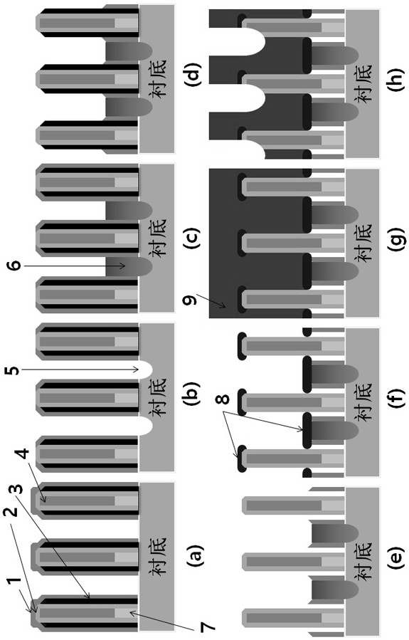
[0021] In the process of forming the air space by using the traditional technology, to achieve the technical effect basically equivalent to that of the present invention, it is necessary to ensure that the process conditions of the film etching selection ratio are sufficiently excellent, and the DRAM operation technology that can control the parasitic capacitance is required. It is very difficult to secure a film quality condition with a low dielectric constant that can control parasitic capacitance. Therefore, the present invention proposes a new solution to form air gaps to solve the problems raised in the background art. In a specific implementation process, an embodiment of the present invention provides a method for forming a bit line air spacer in a semiconductor device manufacturing process, including the following steps:

Embodiment 2

Embodiment 3


PUM


Abstract

The invention discloses a method for forming a bit line air gap in a semiconductor device manufacturing process, which belongs to the field of semiconductor manufacturing, and comprises the following steps of: after forming bit lines in the semiconductor device manufacturing process, sequentially depositing SiN/C/SiN on the bit lines to form three layers of films, forming connecting grooves between the bit lines, and forming the air gap between the bit lines; filling the connecting groove to form contact; the outermost SiN layer in the SiN/C/SiN layers deposited on the side wall of the bit line is removed, so that the C layer in the SiN/C/SiN layers is exposed; then plasma ashing treatment is carried out to remove the C layer so as to form an air gap; and continuously depositing a first metal layer and a second metal layer on the upper part of the formed air opening, and then carrying out patterning treatment to form a bit line air interval. The present invention reduces parasitic capacitance without causing pattern damage, and realizes no additional deposition of a capping film and an air-spaced etching process, thereby minimizing pattern damage.

Description

technical field [0001] The invention relates to the field of semiconductor manufacturing, and more particularly, to a method for forming an air space between bit lines in a semiconductor device manufacturing process. Background technique [0002] In the prior art, in order to improve the performance of DRAM devices, achieve higher-level scaling and faster memory cell operation, and reduce parasitic capacitances, a scheme of arranging air spacers near bit lines has been developed. However, due to the etching selectivity ratio of the film quality and the effect of galvanic corrosion, the bit line may be damaged in this solution. Therefore, a new solution is needed to form an air gap to prevent this phenomenon from happening. SUMMARY OF THE INVENTION [0003] The purpose of the present invention is to overcome the deficiencies of the prior art, and to provide a method for forming an air space between bit lines in a semiconductor device manufacturing process, which can reduce...

Claims


Application Information

Patent Timeline
IPC IPC(8): H01L21/764H01L21/8242
CPCH01L21/764H10B12/482
Inventor 郭炳容
Owner 成都高真科技有限公司
Why Eureka
Try Eureka