
Preparation method of electromagnetic shielding layer

An electromagnetic shielding layer and equipment technology, applied in the direction of copying/marking methods, coatings, circuits, etc., can solve the problems of high cost of PVD coating, unfavorable for PCBA miniaturization, etc., so as to achieve no need for long cycle time and high cost, and reduce materials Waste, simple effect of inkjet process

Inactive Publication Date: 2022-06-28
GIS TECH INC
View PDF0 Cites 0 Cited by
  • Summary
  • Abstract
  • Description
  • Claims
  • Application Information

AI Technical Summary

Problems solved by technology

Adding a metal shell is not conducive to the miniaturization of PCBA, and the cost of PVD coating is relatively high

Method used

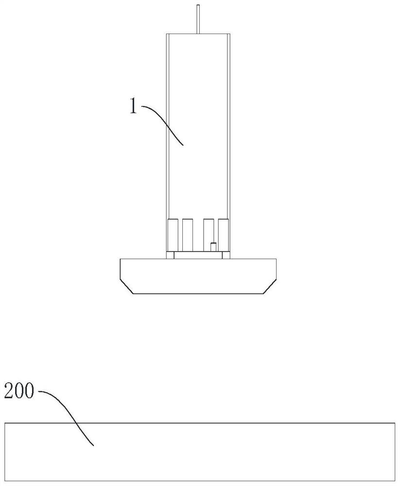
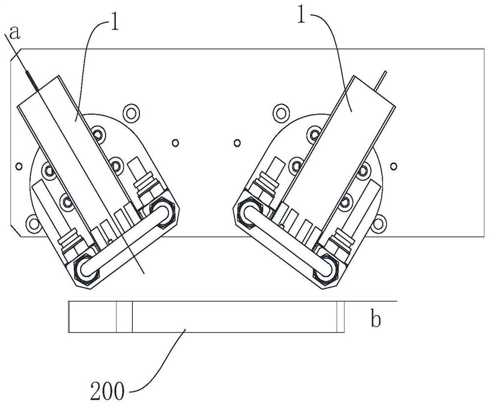
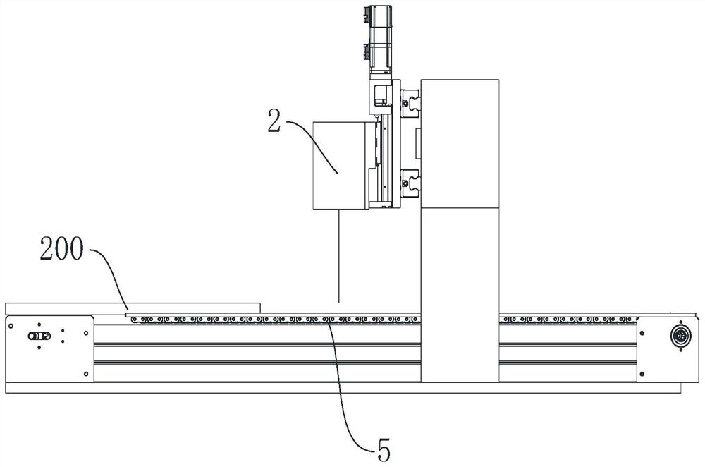

Image

  • Preparation method of electromagnetic shielding layer
  • Preparation method of electromagnetic shielding layer
  • Preparation method of electromagnetic shielding layer

Examples


preparation example Construction

[0030] The application provides a preparation method of an electromagnetic shielding layer, the preparation method comprising:

[0031] S1. Plasma treatment is performed on the surface of the workpiece;

[0032] S2, prepare an insulating layer on the surface of the workpiece;

[0033] S3, using inkjet equipment, according to the inkjet graphic data, inkjet printing to form a spray coating on the surface of the workpiece;

[0034] S4, preparing a protective layer on the spray coating.

[0035] Specifically, the workpiece is a device such as a PCBA board or an FPC board welded with a high-frequency and high-speed semiconductor processor. It should be noted that the surface of the workpiece includes the surface of the PCBA board and the surface of the semiconductor processor located on the PCBA board.

[0036] Plasma treatment is to bombard the surface of the workpiece with a plasma gun, and the surface of the workpiece will form a concave-convex structure, which reduces the sm...

Embodiment 1

[0073] Step 1, see image 3 , install the workpiece 200 on the working platform 2 with the plasma spray gun 3, after completing the positioning, drive the plasma spray gun 3 to perform surface treatment on the workpiece 200, which is the prior art, and the specific parameters are set according to actual needs.

[0074] Step 2, see Figure 4 , move the workpiece 200 to the working platform 2 on which the glue dispenser 4 is installed, and after the positioning is completed, drive the glue dispenser 4 to perform insulation coating on the pair. The specific operation is in the prior art, and will not be repeated here.

[0075] Step 3, see Figure 5 , the workpiece 200 moves on the working platform 2 of the inkjet printing device 100, starts the inkjet printing device 100, and prints the spray coating on the surface and side of the workpiece 200 according to the inkjet graphic data and solidifies, and the method for printing and curing the spray coating is as described above. ,N...


PUM


Abstract

The invention relates to a preparation method of an electromagnetic shielding layer. The preparation method comprises the following steps: S1, carrying out plasma treatment on the surface of a workpiece; s2, preparing an insulating layer on the surface of the workpiece; s3, ink-jet printing is conducted on the surface of the workpiece through ink-jet equipment according to the ink-jet graphic data to form a spraying layer; and S4, a protective layer is prepared on the spraying layer. The electromagnetic shielding layer is prepared through the ink-jet printing technology, electromagnetic shielding protection can be carried out on the local part of the workpiece according to needs, the pattern obtained through ink-jet printing is an actually-needed protection area, material waste is reduced, and precise protection is achieved; meanwhile, aiming at the requirements of different electromagnetic shielding processes, different metal inks can be combined and used for printing different shielding layers; compared with a metal shell electromagnetic shielding process, the ink jet process meets the requirement of miniaturization development of workpieces; compared with a PVD coating process, the ink jet process is simpler, does not need long cycle time and high cost, is more suitable for a smaller area, and can reduce the total cost by about 25% on year-on-year basis.

Description

technical field [0001] The invention relates to a preparation method of an electromagnetic shielding layer. Background technique [0002] With the continuous development and application of high-speed chips, the signal frequency is getting higher and higher, and the printed circuit boards (PCBs) or flexible circuit boards (FPCs) that carry them may become smaller and smaller, so that the integration of IC devices increases with the the improvement. The miniaturization of equipment and the increasing speed of devices have made the problem of electromagnetic interference (EMI) in electronic products more serious. [0003] PCBA is welded with high-frequency and high-speed semiconductor processors, such as FPGA, CPU, IGBT and other electronic components. When such electronic components are working, they do not want to be interfered by external electromagnetic waves, and at the same time, they do not want to radiate electromagnetic waves themselves to interfere with external inte...

Claims


Application Information

Patent Timeline
IPC IPC(8): B05D3/14B05D7/24B05D1/00B05D1/26B41M5/00B41M7/00H01L23/552
CPCB05D3/142B05D7/24B05D1/60B05D1/26B41M5/0047B41M7/0027B41M5/0023H01L23/552
Inventor 覃勇吴景舟马迪
Owner GIS TECH INC
Learn More