Desaturation protection improved circuit suitable for SiC MOSFET, design method and application

A design method and protection circuit technology, applied in emergency protection circuit devices, electrical components, etc., can solve the problems of small chip area, anti-interference effect, high cost, etc., to achieve improved response speed, comprehensive optimization range, and accelerated protection speed Effect

Pending Publication Date: 2022-06-28
深圳市优联半导体有限公司 +1
View PDF0 Cites 0 Cited by
  • Summary
  • Abstract
  • Description
  • Claims
  • Application Information

AI Technical Summary

Problems solved by technology

[0010] (1) SiC MOSFET is limited by a relatively small chip area, and the short-circuit withstand time is significantly shorter than that of Si-based devices, only 2μ s However, the design requirements for SiC MOSFET protection circuits are more stringent, and the response speed of some existing protection circuits cannot fully meet the requirements
[0011] (2) The existing circuit design for SiC MOSFET protection is relatively complex, and the anti-interference performance of the circuit is affected to a certain extent, or the optimization effect is only effective for a single fault type, etc., and there is room for improvement.
[0012] (3) In the existing optimization strategies for desaturation protection schemes, the circuit structure is relatively complex and the cost is relatively high; at the same time, the types of faults that can be handled are limited, or the anti-interference performance will also be affected, etc.

Method used


Image

  • Desaturation protection improved circuit suitable for SiC MOSFET, design method and application
  • Desaturation protection improved circuit suitable for SiC MOSFET, design method and application
  • Desaturation protection improved circuit suitable for SiC MOSFET, design method and application

Examples


Embodiment Construction

[0083] In order to make the objectives, technical solutions and advantages of the present invention clearer, the present invention will be further described in detail below with reference to the embodiments. It should be understood that the specific embodiments described herein are only used to explain the present invention, but not to limit the present invention.

[0084] Aiming at the problems existing in the prior art, the present invention provides an improved desaturation protection circuit suitable for SiC MOSFET, a design method and an application. The present invention is described in detail below with reference to the accompanying drawings.

[0085] 1. Explain the embodiment. In order for those skilled in the art to fully understand how the present invention is specifically implemented, this part is an explanatory embodiment for expanding the description of the technical solutions of the claims.

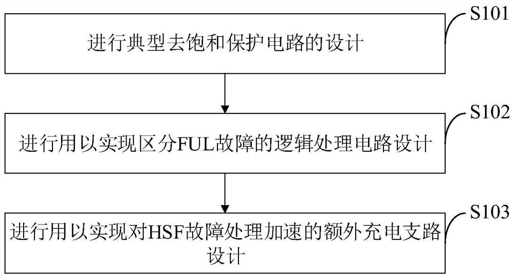
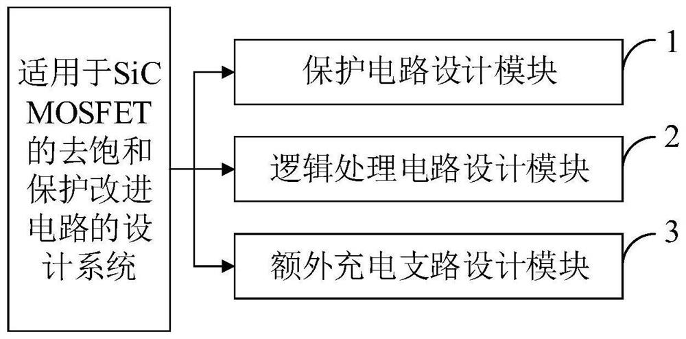
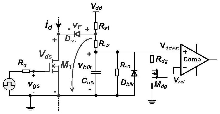
[0086] like figure 1 As shown, the design method of the improved cir...


PUM


Abstract

The invention belongs to the technical field of circuit design, and discloses a desaturation protection improved circuit suitable for a SiC MOSFET, a design method and application, and the desaturation protection improved circuit suitable for the SiC MOSFET comprises a typical desaturation protection circuit topology, a logic processing circuit used for distinguishing FUL faults, and a blanking capacitor charging branch circuit additionally led out from a MOSFET drain electrode. The design method of the desaturation protection improved circuit suitable for the SiC MOSFET comprises the steps that a typical desaturation protection circuit topology is added with a logic processing circuit used for distinguishing FUL faults, then a blanking capacitor charging branch circuit additionally led out from an MOSFET drain electrode is added, and HSF fault processing is accelerated. According to the method, the anti-interference performance is not sacrificed while the response speed is increased, the optimization range is relatively comprehensive, improvement is achieved when two different short-circuit faults are processed, and rapid and reliable circuit protection can be achieved.

Description

technical field [0001] The invention belongs to the technical field of circuit design, and in particular relates to an improved circuit for desaturation protection suitable for SiC MOSFET, a design method and application. Background technique [0002] In recent years, the main development trend of power electronic devices is to continuously pursue higher power density and try to work in a higher temperature environment to meet the needs of various emerging applications, such as electric vehicles and wind power systems. Thanks to advances in material science and production processes, wide-bandgap semiconductor devices such as SiC MOSFETs are beginning to find application in the industry. Compared with traditional Si-based devices, SiC MOSFETs have many advantages, such as high breakdown field strength, high thermal conductivity and high forbidden band width. Therefore, various wide-bandgap semiconductor devices represented by SiC MOSFETs will gradually replace various Si-bas...

Claims


Application Information

Patent Timeline
Patent Type & Authority Applications(China)
IPC IPC(8): H02H7/20
CPCH02H7/205
Inventor 王智强李佳炜辛国庆时晓洁
Owner 深圳市优联半导体有限公司
Why Eureka
Try Eureka