Check patentability & draft patents in minutes with Patsnap Eureka AI!

Shield gate groove type field effect transistor with variable doping concentration structure and preparation method of shield gate groove type field effect transistor

A field-effect transistor and doping concentration technology, which is applied in semiconductor/solid-state device manufacturing, semiconductor devices, electrical components, etc., can solve problems such as high peak voltage, achieve peak electric field improvement, reduce specific on-resistance, and increase breakdown voltage Effect

Pending Publication Date: 2022-07-12
无锡先瞳半导体科技有限公司
View PDF0 Cites 0 Cited by
  • Summary
  • Abstract
  • Description
  • Claims
  • Application Information

AI Technical Summary

Problems solved by technology

[0004] In the SGT device, due to the electric field concentration effect and the high doping concentration of polysilicon in the shield gate, when the SGT device is forward-blocked, the charge flux emitted by the ionized donor in the withstand voltage region is concentrated in the trench region shield At the corner of the gate, the peak voltage at the corner of the shield gate in the trench area is higher, and it is easier to be broken down here

Method used


Image

  • Shield gate groove type field effect transistor with variable doping concentration structure and preparation method of shield gate groove type field effect transistor
  • Shield gate groove type field effect transistor with variable doping concentration structure and preparation method of shield gate groove type field effect transistor
  • Shield gate groove type field effect transistor with variable doping concentration structure and preparation method of shield gate groove type field effect transistor

Examples


Embodiment 1

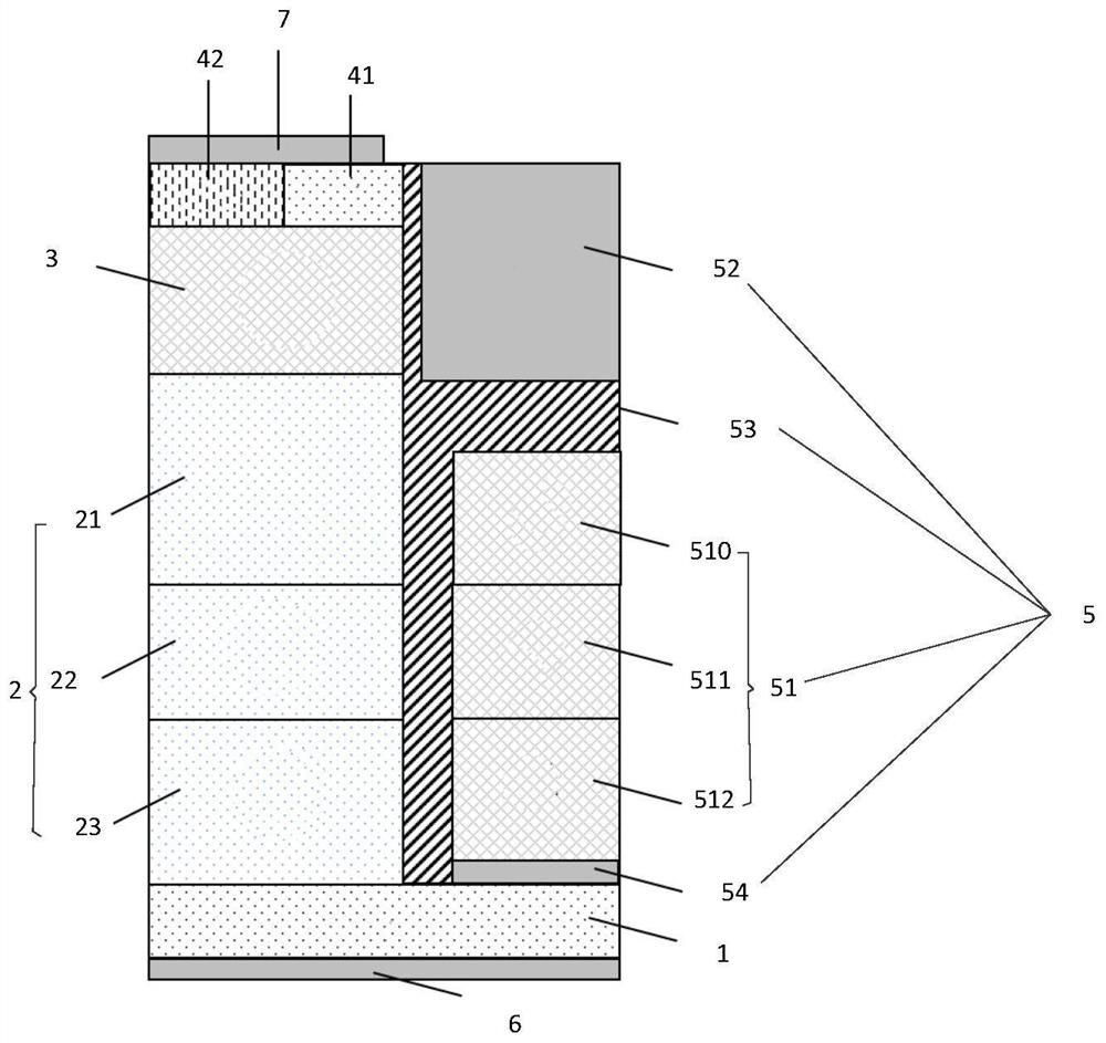
[0045] In the SGT device, due to the high doping concentration of the shielded gate drift region, when the SGT device is blocked in the forward direction, a depletion region is formed between the interface between the drift region and the base region, and a peak electric field exists in the depletion region. The peak electric field can cause breakdown at the corner between the trench region and the drift region due to the electric field concentration effect.

[0046] Therefore, in order to balance the peak electric field in the depletion region, the electric field peak value is more improved, the breakdown voltage is increased, and the specific on-resistance is reduced. Embodiments of the present application provide a shielded gate trench field effect transistor with a variable doping concentration structure.

[0047] figure 1 It is a schematic structural diagram of the shielded gate trench field effect transistor with the variable doping concentration structure shown in the ...

Embodiment 2

[0064] In SGT devices, due to the electric field concentration effect and the high polysilicon doping concentration of the shielding gate, when the SGT device is blocked in the forward direction, the parasitic capacitance formed between the shielding gate and the substrate region is large, which reduces the switching speed of the transistor. .

[0065] Therefore, in order to improve the withstand voltage capability of the SGT device, it is necessary to weaken the electric field strength at the corners of the shield gate in the trench region. Embodiments of the present application provide a shielded gate trench field effect transistor with a variable doping concentration structure.

[0066] figure 1 It is a schematic structural diagram of the shielded gate trench field effect transistor with the variable doping concentration structure shown in the embodiment of the present application.

[0067] see figure 1 , the shielded gate trench field effect transistor of the variable d...

Embodiment 3

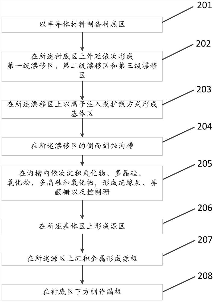
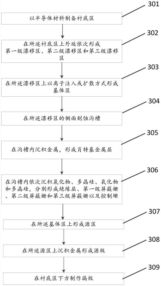
[0083] Corresponding to the shielded gate trench field effect transistor of the variable doping concentration structure shown in the first embodiment, the present application also provides a method for preparing the shielded gate trench field effect transistor of the variable doping concentration structure and the same Corresponding example.

[0084] figure 2 It is a schematic flowchart of a method for fabricating a shielded gate trench field effect transistor with a variable doping concentration structure according to an embodiment of the present application.

[0085] like figure 2 As shown, the method for fabricating the shielded gate trench field effect transistor shown in the embodiment of the present application includes the following steps:

[0086] 201. Prepare a substrate region with a semiconductor material;

[0087] In the embodiment of the present application, the substrate region is prepared with N-type heavily doped semiconductor material, that is, the doping...


PUM


Abstract

The invention relates to a shield gate groove type field effect transistor with a variable doping concentration structure. The shield gate groove type field effect transistor comprises a substrate region, a drift region, a base body region, a source region, a groove region, a drain electrode and a source electrode, the trench region comprises a shield gate, a control gate, an insulating layer and a metal gate; the shield grid and the drift region are of a variable doping concentration structure, the doping concentration of the drift region is gradually reduced from top to bottom, and the doping concentration of the shield grid is gradually reduced from top to bottom. When the transistor is blocked in the forward direction, the electric field between the third-stage drift region and the corner of the trench region is weakened. Therefore, the shield gate trench type field effect transistor with the variable doping concentration structure can balance the peak electric field of the voltage withstanding layer at the interface of the substrate region and the drift region, so that the peak value of the electric field is improved, the breakdown voltage is improved, and the specific on-resistance is reduced.

Description

technical field [0001] The present application relates to the technical field of power semiconductor devices, and in particular, to a shielded gate trench field effect transistor with a variable doping concentration structure and a preparation method thereof. Background technique [0002] Shielded gate trench field effect transistors (Split Gate Trench, SGT) have been widely used in important low-voltage fields such as power management. SGT has high channel density and good charge compensation effect. In addition, the shielded gate structure effectively isolates the coupling between the control gate and the drain, thereby significantly reducing the transfer capacitance. [0003] Therefore, SGT has lower specific on-resistance, smaller conduction and switching losses, and higher operating frequency. [0004] In the SGT device, due to the electric field concentration effect and the high polysilicon doping concentration of the shielding gate, when the SGT device is blocked in...

Claims


Application Information

Patent Timeline
IPC IPC(8): H01L29/49H01L29/06H01L29/78H01L21/336
CPCH01L29/4925H01L29/0623H01L29/7813H01L29/7811H01L29/66734
Inventor 张子敏王宇澄虞国新吴飞钟军满
Owner 无锡先瞳半导体科技有限公司
Features
  • R&D
  • Intellectual Property
  • Life Sciences
  • Materials
  • Tech Scout
  • Unparalleled Data Quality
  • Higher Quality Content
  • 60% Fewer Hallucinations
Learn More