Strip for circuits having rose gold contact pad and method for manufacturing the strip

A technology of electrical contact pads and strips, which is applied to record carriers, instruments, and calculations used by machines, and can solve problems such as doubtful quality

Pending Publication Date: 2022-07-12
LINXENS HLDG SAS
View PDF1 Cites 0 Cited by
  • Summary
  • Abstract
  • Description
  • Claims
  • Application Information

AI Technical Summary

Problems solved by technology

However, the production of electrical contact pads in new colors must not have their quality in doubt, e.g. in terms of contact resistance, resistance to climate tests, corrosion resistance, fatigue resistance, etc.

Method used


Image

  • Strip for circuits having rose gold contact pad and method for manufacturing the strip
  • Strip for circuits having rose gold contact pad and method for manufacturing the strip
  • Strip for circuits having rose gold contact pad and method for manufacturing the strip

Examples


Embodiment Construction

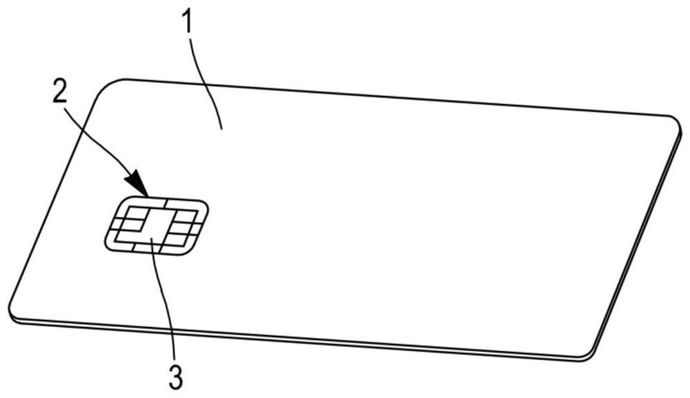
[0013] A disclosed example of a circuit made from a strip according to the invention is described below. This example is taken from the field of smart cards, but those skilled in the art will be able to transfer this example to other circuit applications without involving inventive step. In particular, the present invention is particularly beneficial where the use of all pink conductive contacts or pink conductive traces may bring an aesthetic added value (for example to a connector for an SD memory card or a connector for a USB memory stick).

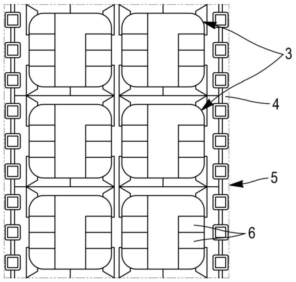
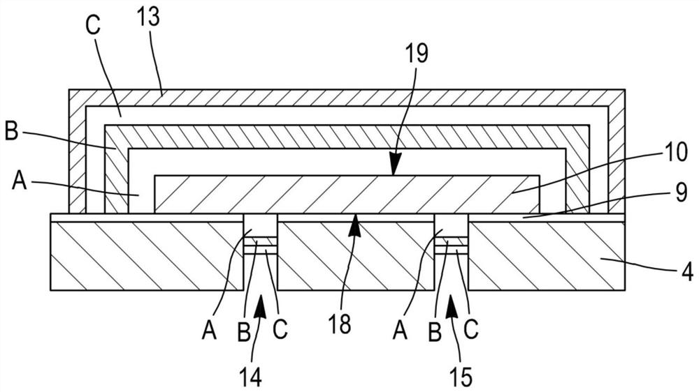
[0014] like figure 1 As shown, the smart card 1 comprises, for example, a module 2 with a connector 3 . The modules 2 are usually made in the form of individual elements cut from strips. This element is inserted into a cavity formed in the card 1 . The element comprises a substantially flexible substrate 4 made of polyethylene terephthalate (PET), glass-epoxy, etc. (see figure 2 ), a connector 3 is formed on the substrate 4, and t...


PUM


Abstract

The invention relates to a strip for producing an electrical circuit with electrical contact pads, comprising:-a flexible dielectric substrate (4),-a copper foil (10) at least partially covering the dielectric substrate (4), the copper foil (10) having an inner face (18) facing the dielectric substrate (4) and an outer face (19) opposite the inner face (18),-an intermediate layer, the intermediate layer comprises at least a nickel-based layer at least partially covering the outer face (19) of the copper foil (10), and a gold-copper alloy layer (13) is deposited on the intermediate layer. A method of manufacturing an electrical circuit includes providing a strip having a conductive pad, and plating the pad with a gold-copper alloy layer electrodeposited from an electrodeposition solution.

Description

technical field [0001] The present invention relates to circuits having contact pads. For example, the circuit is used to manufacture a smart card module comprising electrical contact pads designed to be connected to a connector of a smart card reader (the smart card is used for eg banking applications and identification documents). Background technique [0002] A connector module for a smart card comprises a dielectric substrate supporting electrical contact pads (see eg document WO2019051712A1). Electrical contact pads are etched (by, for example, photolithographic techniques and etching techniques) in a conductive layer supported by a flexible dielectric substrate. Alternatively, the electrical contact pads are cut out of the conductive layer and then co-laminated on a flexible dielectric substrate (by eg lead frame technology). In both cases, the contact pads supported by the dielectric substrate are made as flexible strips. More generally, such flexible strips with e...

Claims


Application Information

Patent Timeline
IPC IPC(8): C25D3/62C25D5/02C25D5/12C25D5/56C25D7/00C23F1/00G06K19/077
CPCC25D3/62C25D5/022C25D5/12C25D5/56C25D7/00G06K19/07743C23F1/02G06K19/07718C25D5/627
Inventor 弗洛里安·万诺斯蒂芬尼·柯奎拉德
Owner LINXENS HLDG SAS
Why Eureka
Try Eureka