Reference clock abnormity self-checking circuit and method
A technology of reference clock and self-checking circuit, applied in multiple input and output pulse circuits, electrical components, detecting faulty computer hardware, etc., can solve the problem of long logic judgment time, sub-system inoperable, and too late to give switching signal and other problems to achieve the effect of increasing reliability
- Summary
- Abstract
- Description
- Claims
- Application Information
AI Technical Summary
Problems solved by technology
Method used
Image

Examples
Embodiment 1
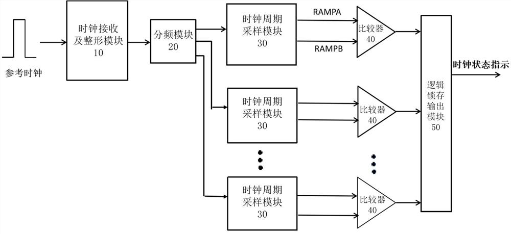
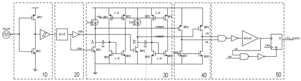
[0040] figure 1 It is a schematic block diagram of the reference clock abnormality self-checking circuit according to the present application, such as figure 1 As shown, the reference clock abnormality self-checking circuit of the present application includes a clock receiving and shaping module 10 , a frequency dividing module 20 , a clock cycle sampling module 30 , a comparator 40 , and a logic latch output module 50 .
[0041] The clock receiving and shaping module 10 , which performs denoising and shaping processing on the received reference clock signal and sends it to the frequency dividing module 20 .
[0042] In the embodiment of the present application, the clock receiving and shaping module 10 uses a Schmitt trigger with hysteresis to perform denoising and shaping processing on the reference clock signal.
[0043] The frequency dividing module 20 divides the frequency of the reference clock signal after denoising and shaping to obtain a reference clock cycle signal ...
Embodiment 2
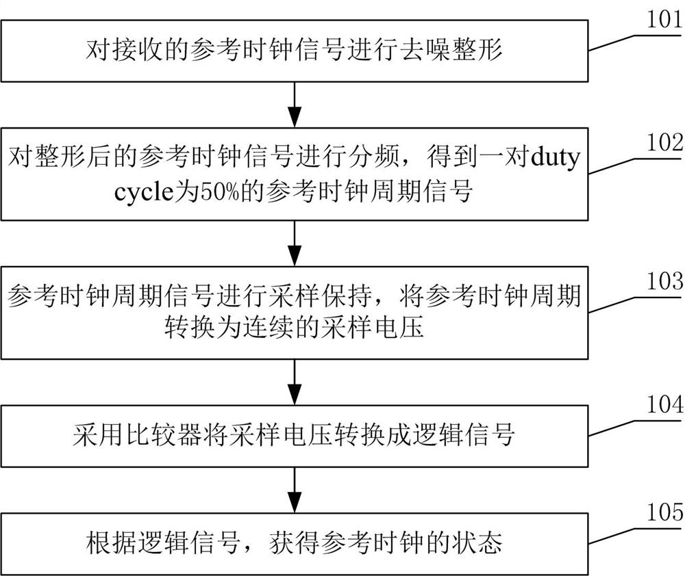
[0073] image 3 For the flow chart of the reference clock anomaly detection method according to the present application, the following will refer to image 3 , the reference clock anomaly detection method of the present application is described in detail.
[0074] First, in step 101, the received reference clock signal is denoised and shaped.
[0075] In the embodiment of the present application, the clock receiving and shaping module 10 with a Schmitt trigger with hysteresis is used to de-noise and shape the reference clock signal.
[0076] In step 102, the frequency of the shaped reference clock signal is divided to obtain a reference clock period signal.
[0077] In the embodiment of the present application, the frequency dividing module 20 is used to divide the frequency of the reference clock signal to obtain a pair of reference clock cycle signals whose dutycycle is 50%.
[0078] In step 103, the frequency-divided reference clock period signal is sampled and held, and...
Embodiment 3
[0088] The present application also provides a micro-control chip, including the above-mentioned abnormal self-checking circuit of the reference clock.
[0089] In the embodiments of this application, micro-control chips include but are not limited to processors for consumer electronic products, processors for industrial products such as smart home, automation, medical applications, and new energy generation and distribution, and automotive-grade MCU chips for automotive electronics Wait.
PUM
 Abstract
Description
Claims
Application Information
 - R&D
- Intellectual Property
- Life Sciences
- Materials
- Tech Scout
- Unparalleled Data Quality
- Higher Quality Content
- 60% Fewer Hallucinations
Browse by: Latest US Patents, China's latest patents, Technical Efficacy Thesaurus, Application Domain, Technology Topic, Popular Technical Reports.
© 2025 PatSnap. All rights reserved.Legal|Privacy policy|Modern Slavery Act Transparency Statement|Sitemap|About US| Contact US: help@patsnap.com