Light emitting diode epitaxial wafer and manufacturing method thereof

A technology for light-emitting diodes and a manufacturing method, which is applied to semiconductor devices, electrical components, circuits, etc., can solve the problems of low luminous efficiency and uneven wavelength uniformity of light-emitting diodes, and achieve improved lattice quality, uniform distribution, and tight fit. Effect

Active Publication Date: 2022-07-29
JIANGXI ZHAO CHI SEMICON CO LTD
View PDF4 Cites 5 Cited by
  • Summary
  • Abstract
  • Description
  • Claims
  • Application Information

AI Technical Summary

Problems solved by technology

[0005] Based on this, the object of the present invention is to provide a light-emitting diode epitaxial wafer and its manufacturing method to fundamentally solve the problems of low luminous efficiency and low wavelength uniformity of existing light-emitting diodes.

Method used


Image

  • Light emitting diode epitaxial wafer and manufacturing method thereof
  • Light emitting diode epitaxial wafer and manufacturing method thereof
  • Light emitting diode epitaxial wafer and manufacturing method thereof

Examples


Embodiment 1

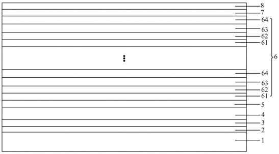
[0041] see figure 1 , is a schematic structural diagram of a light-emitting diode epitaxial wafer provided by the first embodiment of the present invention. For the convenience of description, only the part related to the embodiment of the present invention is shown. The light-emitting diode epitaxial wafer provided by the embodiment of the present invention includes:

[0042] A substrate 1, and a buffer layer 2, an undoped u-GaN layer 3, an N-type GaN layer 4, a stress release layer 5, a multiple quantum well layer 6, an electron blocking layer 7, and a P type GaN layer 8;

[0043] The multiple quantum well layer 6 includes a front insertion layer 61, a quantum well layer 62, a rear insertion layer 63 and a quantum barrier layer 64 that are periodically and repeatedly stacked;

[0044] The front insertion layer 61 includes laminated In x N 1-x Layer and In y Ga 1-y N layer, In x N 1-x Layer and In y Ga 1-y The surface contacted by the N layer is also subjected to H ...

Embodiment 2

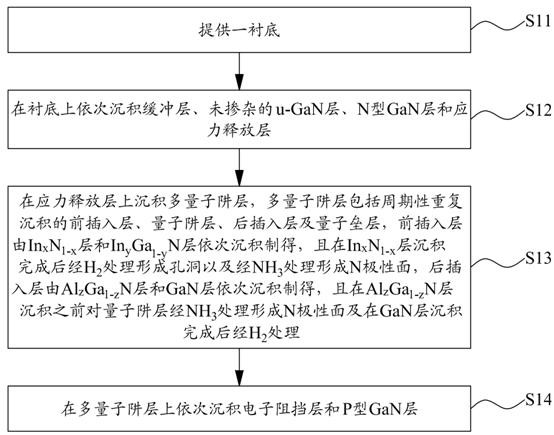
[0065] see figure 2 , shows a method for fabricating a light-emitting diode epitaxial wafer in the second embodiment of the present invention, and the method specifically includes steps S11 to S14 .

[0066] Step S11, providing a substrate.

[0067] Wherein, in the embodiments of the present invention, the selected substrates include but are not limited to sapphire substrates, silicon substrates, silicon carbide substrates, aluminum nitride substrates, gallium nitride substrates, and substrates such as silicon dioxide and sapphire. The composite substrate composed of, specifically, in this embodiment, sapphire is used as the epitaxial layer growth substrate, which can make a periodically changing structure on the substrate to form a patterned substrate, or SiO can be used 2 -Al 2 O 3 and other composite patterned substrates. Specifically, in the embodiment of the present invention, a sapphire patterned substrate is used as the epitaxial layer growth substrate.

[0068] F...


PUM

PropertyMeasurementUnit
thicknessaaaaaaaaaa
thicknessaaaaaaaaaa
thicknessaaaaaaaaaa

Abstract

The invention provides a light emitting diode epitaxial wafer and a manufacturing method thereof. The epitaxial wafer comprises a substrate, a buffer layer, an undoped u-GaN layer, an N-type GaN layer, a stress release layer, a multi-quantum well layer, an electron barrier layer and a P-type GaN layer, the multi-quantum well layer comprises a front insertion layer, a quantum well layer, a rear insertion layer and a quantum barrier layer; the front insertion layer comprises an In < x > N < 1-x > layer and an In < y > Ga < 1-y > N layer, and the contact surface of the In < x > N < 1-x > layer and the In < y > Ga < 1-y > N layer is processed by H2 to form a hole and processed by NH3 to form an N polar surface; the rear insertion layer comprises an Al < z > Ga < 1-z > N layer and a GaN layer, the surface, in contact with the Al < z > Ga < 1-z > N layer, of the quantum well layer is subjected to NH3 treatment to form an N polar surface, and the surface, in contact with the quantum barrier layer, of the GaN layer is subjected to H2 treatment. According to the invention, the problems of low luminous efficiency and low wavelength uniformity of the existing light-emitting diode are solved.

Description

technical field [0001] The invention relates to the field of optoelectronic technology, in particular to a light emitting diode epitaxial wafer and a method for making the same. Background technique [0002] At present, GaN-based light-emitting diodes have been widely used in the field of solid-state lighting and display, attracting more and more people's attention. GaN-based light-emitting diodes have been industrially produced and have applications in backlights, lighting, landscape lights, etc. [0003] As the core structure of the light-emitting diode, the multiple quantum well layer is the key structure that affects the uniformity of the light-emitting wavelength and the light-emitting efficiency. The internal defects of the multiple quantum well layer lead to more non-radiative recombination, which is the problem to be solved for the luminous efficiency of light-emitting diodes to continue to improve; and the high In composition doping leads to the segregation of In c...

Claims


Application Information

Patent Timeline
Patent Type & Authority Applications(China)
IPC IPC(8): H01L33/06H01L33/22H01L33/24H01L33/32H01L33/00
CPCH01L33/06H01L33/22H01L33/24H01L33/325H01L33/0075H01L33/0095H01L33/0066
Inventor 张彩霞印从飞程金连胡加辉金从龙
Owner JIANGXI ZHAO CHI SEMICON CO LTD
Why Eureka
Try Eureka